Solid-state image pickup device, method of manufacturing the same and electronic apparatus

a pickup device and solid-state technology, applied in the direction of television systems, transistors, radio-controlled devices, etc., can solve the problems of limited light-gathering, difficult to gather light on the long wavelength side, and existing configurations that may not achieve sufficient pupil correction, etc., to achieve efficient light-introduction

Active Publication Date: 2012-07-17
SONY SEMICON SOLUTIONS CORP
View PDF6 Cites 37 Cited by
  • Summary
  • Abstract
  • Description
  • Claims
  • Application Information

AI Technical Summary

Benefits of technology

[0007]Accordingly, it is desirable to make it possible to effectively introduce light to an optical waveguide and lead it to a light-receiving portion even if the cell size of the light-receiving portion is reduced.
[0009]In the embodiments of the present invention as described above, since the rectangular lens is formed of the same material as that of the second waveguide core portion and is provided integrally with the second waveguide core portion, optical diffraction of the rectangular lens can efficiently lead light into the waveguide.
[0016]According to the embodiments of the present invention, it is possible for the rectangular lens disposed at the upper end of the optical waveguide to efficiently introduce light into the optical waveguide and lead it to the light-receiving portion.

Problems solved by technology

However, the related art has the following problem.
As a cell size is reduced, a spherical lens (refraction type) causes a limitation of light-gathering.
In particular, it is difficult to gather light on the long wavelength side.
In addition, if pupil correction is intended to be performed by a lens provided at the upper end of the optical waveguide, a problem occurs in which the existing configuration may not achieve sufficient pupil correction due to a problem of a gap between adjacent cells.

Method used


Image

  • Solid-state image pickup device, method of manufacturing the same and electronic apparatus
  • Solid-state image pickup device, method of manufacturing the same and electronic apparatus
  • Solid-state image pickup device, method of manufacturing the same and electronic apparatus

Examples


Embodiment Construction

[0030]Preferred embodiments of the present invention will be described with reference to the drawings. Incidentally, the description is given in the following order.

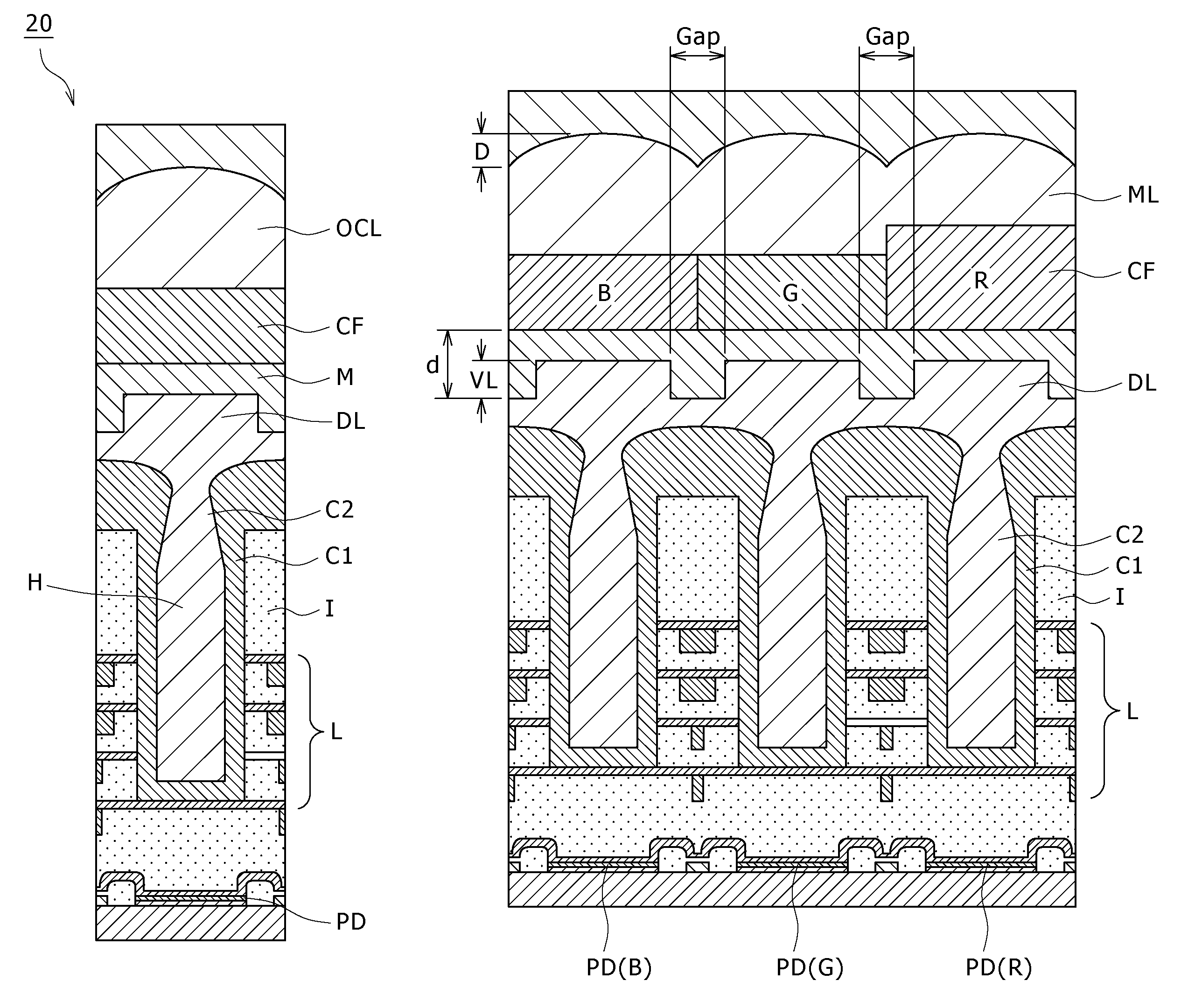
[0031]1. A configuration of a solid state image pickup device (an example of a main portion planar configuration and an example of a sectional configuration)

[0032]2. A method of manufacturing the solid-state image pickup device (examples of first and second manufacturing methods)

[0033]3. Light-receiving sensitivity simulations (simulation calculation examples of effects of light-receiving sensitivity and of pupil correction)

[0034]4. An electric apparatus (an example of application to an image-pickup apparatus)

[A Major Portion Planar Configuration of the Solid-State Image Pickup Device According to an Embodiment]

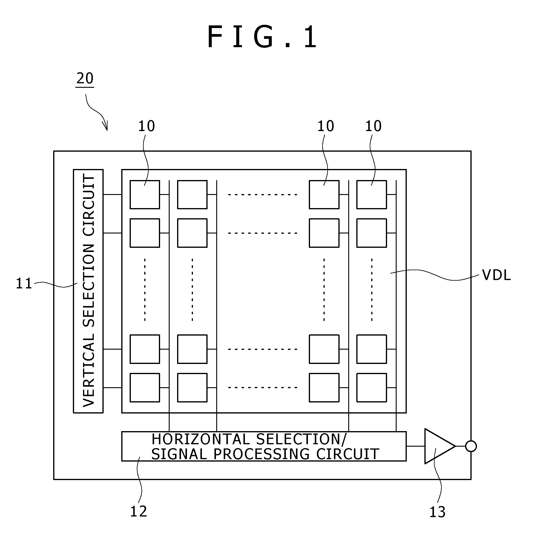
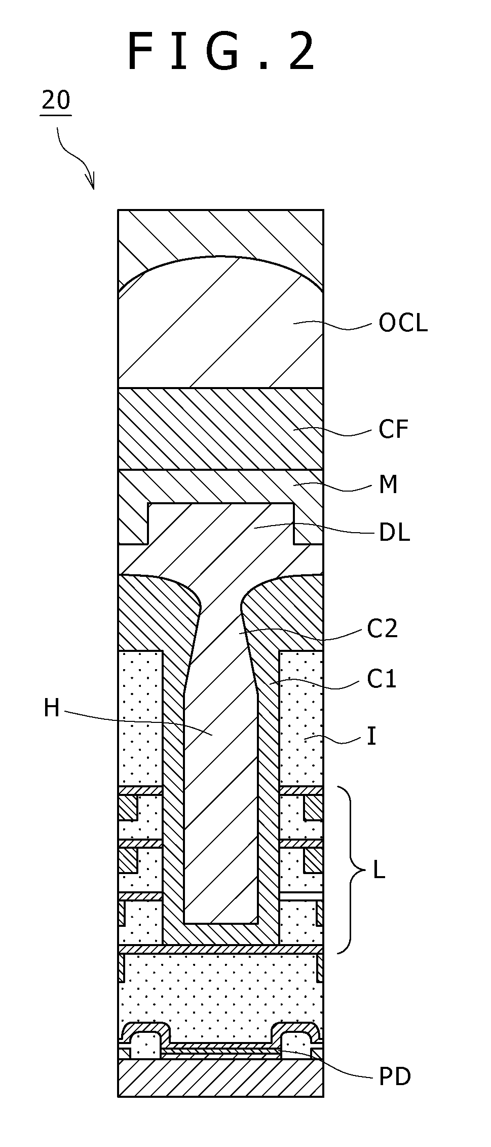
[0035]FIG. 1 is a schematic plan view for assistance in explaining an example of a solid-state image sensor which is a major portion of the solid-state image pickup device according to the present embodiment. A so...


PUM


Abstract

Disclosed herein is a solid-state image pickup device including: a trench formed in an insulating film above a light-receiving portion; a first waveguide core portion provided on an inner wall side of the trench; a second waveguide core portion filled in the trench via the first waveguide core portion; and a rectangular lens formed of the same material as that of the second waveguide core portion and provided integrally with the second waveguide core portion.

Description

CROSS REFERENCE TO RELATED APPLICATION[0001]The present application claims priority to Japanese Priority Patent Application JP 2009-129784 filed in the Japan Patent Office on May 29, 2009, which is hereby incorporated by reference in its entirety to the extent permitted by law.BACKGROUND OF THE INVENTION[0002]1. Field of the Invention[0003]The present invention relates to a solid-state image pickup device, a method of manufacturing the same and an electronic apparatus. In particular, the present invention relates to a solid-state image pickup device that has optical waveguides in insulating films above a light-receiving portion, a method of manufacturing the same and an electronic apparatus.[0004]2. Description of the Related Art[0005]A solid-state image pickup device decreases in light-gathering power due to miniaturization of a cell which is a unit centering a light-receiving portion. Therefore, in the past the solid-state image pickup device has employed a configuration in which ...

Claims


Application Information

Patent Timeline
Patent Type & Authority Patents(United States)
IPC IPC(8): H01L29/76H01L31/062H01L31/113H01L29/94H01L31/119H01L27/14H01L27/146H04N5/335H04N5/361H04N5/369H04N5/372
CPCH01L27/14621H01L27/14629H01L27/14685H01L27/14627
Inventor OGINO, AKIKOSAYAMA, YUKIHIROSHOYA, TAKAYUKISHIMOJI, MASAYA
Owner SONY SEMICON SOLUTIONS CORP
Why Eureka
Try Eureka