Method of manufacturing liquid crystal display device including forming beveled sides of substrates forming liquid crystal panel

a technology of liquid crystal display and beveled sides, which is applied in the direction of instruments, non-linear optics, optics, etc., can solve the problems of deteriorating image quality, sealing material leakage out of the upper and lower surfaces of glass substrates, etc., and achieves excellent yield, high performance, and the effect of bending the display surfa

Active Publication Date: 2012-07-31
PANASONIC LIQUID CRYSTAL DISPLAY CO LTD +1
View PDF3 Cites 8 Cited by
  • Summary
  • Abstract
  • Description
  • Claims
  • Application Information

AI Technical Summary

Benefits of technology

[0010]The present invention has been made to solve the problems of the conventional technology. An object of the present invention is to provide a method of manufacturing a liquid crystal display device in which a glass substrate is uniformly thinned by chemical polishing, breaking of glass or remaining of bubbles during subsequent polarizing plate bonding is prevented, an excellent yield and a high performance are obtained, and a display surface can be bent.
[0019]The glass substrate can be uniformly thinned by chemical polishing. Therefore, it is possible to manufacture a liquid crystal display device in which the breaking of glass or the remaining of bubbles during subsequent polarizing plate bonding is prevented, an excellent yield and a high performance are obtained, and a display surface can be bent.

Problems solved by technology

When the glass substrate is thinned and then a liquid crystal injection hole provided in a side surface of the glass substrate is sealed with a sealing material made of a resin, it is likely to cause a defect in which the sealing material leaks out of the upper and lower surfaces of the glass substrate because the glass substrate is thin.
A local thickness difference of the glass substrate causes the breaking of glass or the remaining of bubbles during subsequent polarizing plate bonding, thereby degrading image quality.

Method used


Image

  • Method of manufacturing liquid crystal display device including forming beveled sides of substrates forming liquid crystal panel
  • Method of manufacturing liquid crystal display device including forming beveled sides of substrates forming liquid crystal panel
  • Method of manufacturing liquid crystal display device including forming beveled sides of substrates forming liquid crystal panel

Examples


embodiment 1

[Embodiment 1]

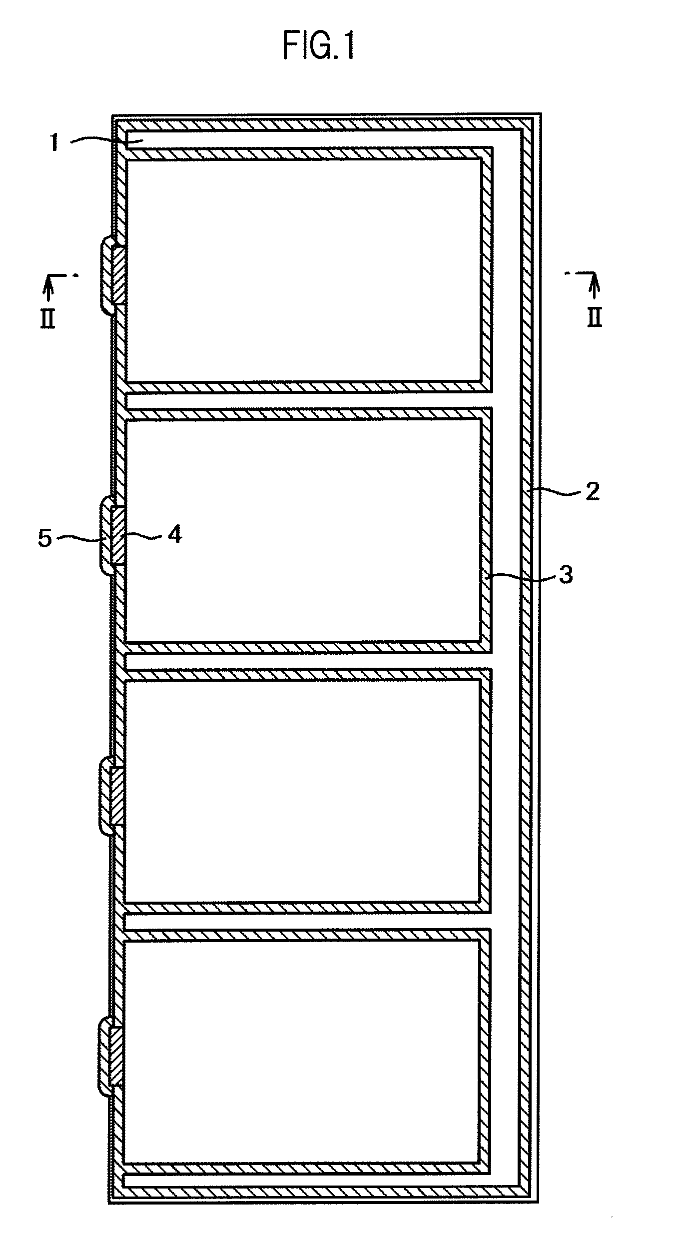
[0030]FIG. 1 illustrates a pair of mother glass substrates in which a plurality of liquid crystal panels are formed. In FIG. 1, 4×1 liquid crystal panels are formed between the pair of mother glass substrates in a strip shape.

[0031]FIG. 1 illustrates a pair of mother glass substrates 1 in which the plurality of liquid crystal panels are formed, a peripheral seal material 2, seal materials surrounding liquid crystals 3, injection holes 4, and sealing materials 5.

[0032]Each of the plurality of liquid crystal panels is formed as follows. The pair of mother glass substrates 1 are bonded to each other with a predetermined gap. A liquid crystal is injected from the injection hole 4 to the predetermined gap surrounded by the seal material 3. The injection hole 4 is sealed with the sealing material 5 made of a resin.

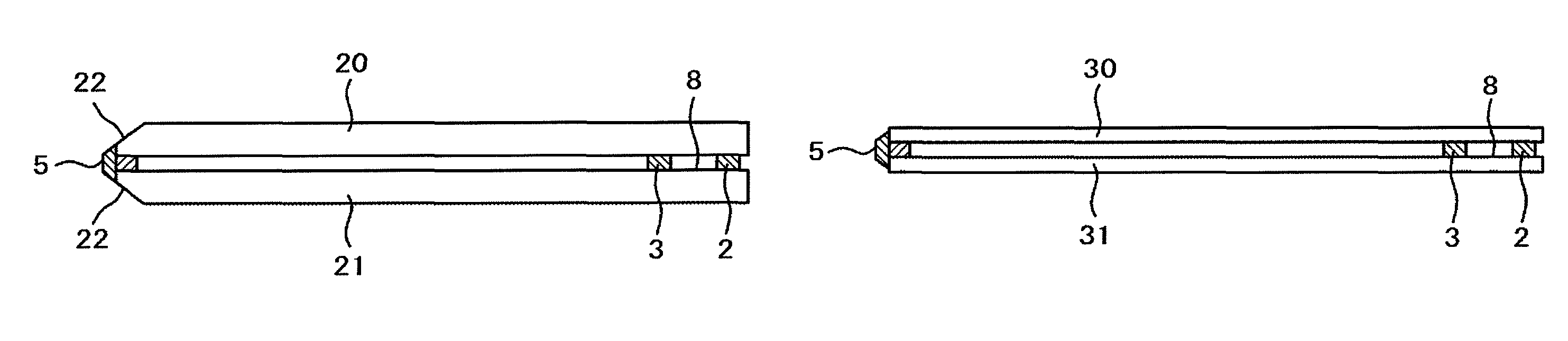
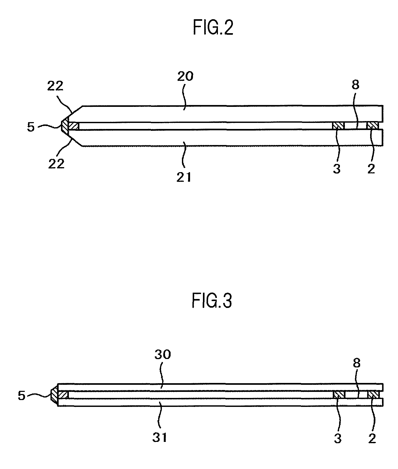
[0033]FIG. 2 is a cross sectional view taken along a line A-A of FIG. 1 before chemical polishing. FIG. 2 illustrates a first glass substrate 21 and a second glass...

embodiment 2

[Embodiment 2]

[0048]FIGS. 5A and 5B illustrate a pair of mother glass substrates according to a structure of Embodiment 2. FIG. 5A is a plan view and FIG. 5B is a cross sectional view taken along a line C-C of FIG. 5A after chemical polishing.

[0049]In Embodiment 2, the terminal portion 8 is exposed in advance. A protective film 9 is formed before chemical polishing to prevent the terminal portion 8 from being brought into contact with the etching solution. The other structures are the same as in Embodiment 1.

[0050]The protective film 9 is removed before the flexible circuit board is connected to the terminal portion. The protective film 9 may be removed before or after the pair of mother glass substrates 1 are cut into the respective liquid crystal panels. The protective film 9 may be an organic resist film or an organic film formed by CVD. The protective film 9 can be removed by chemical cleaning or mechanical peeling.

[0051]Even in this embodiment, the glass substrates can be etche...

embodiment 3

[Embodiment 3]

[0052]FIGS. 6A and 6B illustrate a pair of mother glass substrates according to a structure of Embodiment 3. FIG. 6A is a plan view and FIG. 6B is a cross sectional view taken along a line D-D of FIG. 6A after chemical polishing.

[0053]In this embodiment, the terminal portion 8 is exposed in advance, and then flexible circuit boards 10 are connected to the terminals on the terminal portion 8. The protective film 9 is formed to prevent the terminal portion 8 and the flexible circuit boards 10 from being brought into contact with the etching solution. The other structures are the same as in Embodiments 1 and 2.

[0054]After chemical polishing, respective liquid crystal panels each having a flexible circuit board are obtained by cutting. In this embodiment, it is unnecessary to remove the protective film 9, but the protective film 9 may be removed. The protective film 9 may be formed on the surface of the terminal portion 8 and only surfaces of the flexible circuit boards 10...


PUM

PropertyMeasurementUnit
thicknessesaaaaaaaaaa
thicknessaaaaaaaaaa
thicknessaaaaaaaaaa

Abstract

Provided is a method of manufacturing a liquid crystal display device containing a liquid crystal panel which holds a liquid crystal between first and second glass substrates. The method includes: an injecting step of injecting the liquid crystal from an injection hole for injecting the liquid crystal, which is provided on at least one side of the liquid crystal panel; a sealing step of sealing the injection hole with a sealing material; a beveling step of processing sides of the first glass substrate and the second glass substrate, at which the injection hole is provided, into a shape in which a thickness of each of the sides increases from end portions of the first glass substrate and the second glass substrate toward central portions thereof; and an etching step of etching the first glass substrate and the second glass substrate by chemical polishing.

Description

CROSS-REFERENCE TO RELATED APPLICATION[0001]The present application claims priority from Japanese application JP2008-044664 filed on Feb. 26, 2008, the content of which is hereby incorporated by reference into this application.BACKGROUND OF THE INVENTION[0002]1. Field of the Invention[0003]The present invention relates to a method of manufacturing a liquid crystal display device, and more particularly, to a method of manufacturing a liquid crystal display device used as a flexible display in which a glass substrate is thinned and a display surface can be bent.[0004]2. Description of the Related Art[0005]A liquid crystal display panel contained in a liquid crystal display device is an image display device which fundamentally includes a liquid crystal layer injected between a first substrate and a second substrate, each being suitably a glass substrate, and which is based on the fact that the alignment direction of a liquid crystal is changed according to an electric field applied to ...

Claims


Application Information

Patent Timeline
Patent Type & Authority Patents(United States)
IPC IPC(8): G02F1/1339G02F1/1341
CPCG02F1/1303G02F1/1333G02F1/133305G02F1/133351G02F1/1339G02F1/1341G02F1/1345G02F1/13
Inventor SASAKI, SUSUMUENDO, HIROAKINEMOTO, SOTAYUUKI, MASANORIAZUMA, HITOSHI
Owner PANASONIC LIQUID CRYSTAL DISPLAY CO LTD
Why Eureka
Try Eureka