Method for obtaining field strength information

a field strength and information technology, applied in the field of field strength information and circuit arrangement, can solve the problem of insufficient spatial resolution, and achieve the effect of advantageously determining the field strength of an input signal

Inactive Publication Date: 2012-07-31
ATMEL CORP
View PDF7 Cites 2 Cited by
  • Summary
  • Abstract
  • Description
  • Claims
  • Application Information

AI Technical Summary

Benefits of technology

[0007]It is therefore an object of the present invention to provide a method by means of which the field strength of an input signal can be determined advantageously. A further object of the present invention is to provide a circuit arrangement for carrying out the method.
[0010]An advantage of the method or the circuit arrangement is that the field strength of the particularly received electromagnetic signal can be determined without further calculations in a simple manner from a comparison of the applied gate voltage of a MOS transistor and stored field strength values, already assigned beforehand to the gate voltage. As a result, the method can be used for determining the spatial distance between the receiver unit and a transmitting unit, in that the field strength values, assigned in the value table to the respective gate voltage, are linked to a distance value. In this regard, a distance range within which data transmission is permitted can be established with the values from the value table. Further, the data rate can be increased with a decline in the distance. Further, because of the low power consumption, the method is especially suitable for obtaining field strength information in the case of transponders. The method of the invention is based, inter alia, on the fact that the field strength is linked to the distance between a receiving station and a transmitting station by a nonlinear functional relation and the nonlinear relation is inversely proportional in part to the nonlinear relation of a change in the forward resistance of a MOS transistor, operating within the nonlinear range, preferably in the “subthreshold” range. As a result, both nonlinear dependences are compensated in part, so that the gate voltage is increased or reduced linearly with rising values or declining values of the received field strength or the distance, until the output voltage of the operational amplifier lies within a predefined interval around the reference voltage. Tests by the applicant have shown that the level of the gate voltage in a first approximation is proportional to the logarithm of the distance. Because the amplification of the operational amplifier remains constant, the output voltage of the operational amplifier has a fixed ratio to the input voltage. As a result, the amplification is not increased either at low or at high input voltages and the ratio of the signal voltage to the noise voltage remains low over the entire amplification range. Another important advantage is that, because of the linear dependence of the values of the gate voltage to the distance, there is a uniform spatial resolution by means of the method of the invention both at small distances to the transmitting station and at great distances to the transmitting station.
[0011]Further, particularly with varying signal levels, a rapid turn-on and turn-off transient behavior at the output of the operational amplifier is achieved, because the output voltage and the input voltage of the operational amplifier fluctuate only to a minor extent and the capacitances present at the input or output of the operational amplifier are not recharged and the power consumption is reduced. In particular, in the case of pulse-pause modulated signals, the field gaps can be reduced by the short turn-on and turn-off transient behavior and the data rate increased. Another advantage of the fixed amplification factor is that in the case of the operational amplifier, the amplification can be adjusted precisely with a low current consumption by means of a high-impedance negative feedback. Another advantage of the method is that the nonlinear change in the resistance value of an individual resistance, which is preferably formed as an individual MOS transistor, is sufficient for regulating the input voltage present at the operational amplifier. In contrast, a particular advantage of the MOS transistor in comparison with a bipolar transistor is that the gate of the MOS transistor can be controlled virtually without loss and at low received field strengths a circuit formed in such a way requires little power to determine the received field strength. Specifically in circuits operating passively, i.e., those that draw the needed power exclusively from the electromagnetic field of a transmitting station, this is an important advantage in order to increase the communication range between [sic] a receiver operating according to the method of the invention.
[0012]Further, it is advantageous to supply the input voltage to the operational amplifier from a divider node of an input resistance realized as a voltage divider and hereby to change only the single resistance of the voltage divider part connected to a reference potential.
[0014]In another embodiment, to adjust the operating point or the gate voltage of the MOS transistor, the storage element can be supplied with current from a constant current source. The voltage level of the capacitor and thereby the operating point of the MOS transistor can be adjusted by the constant current source, without currents from the controllable current source or sink being required. In another preferred refinement, the storage element can be discharged by a switching means, preferably realized as a MOS transistor, to be able to adjust rapidly specifically defined voltage conditions or great fluctuations in the received field strength.

Problems solved by technology

Because of the fixedly predefined values of the resistance branches, the spatial resolution is very different depending on the distance; the spatial resolution is insufficient particularly at a short distance.

Method used


Image

  • Method for obtaining field strength information
  • Method for obtaining field strength information
  • Method for obtaining field strength information

Examples


Embodiment Construction

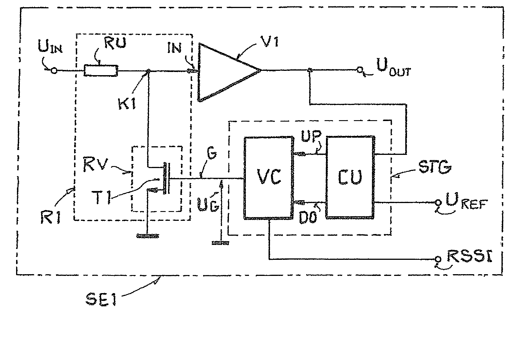
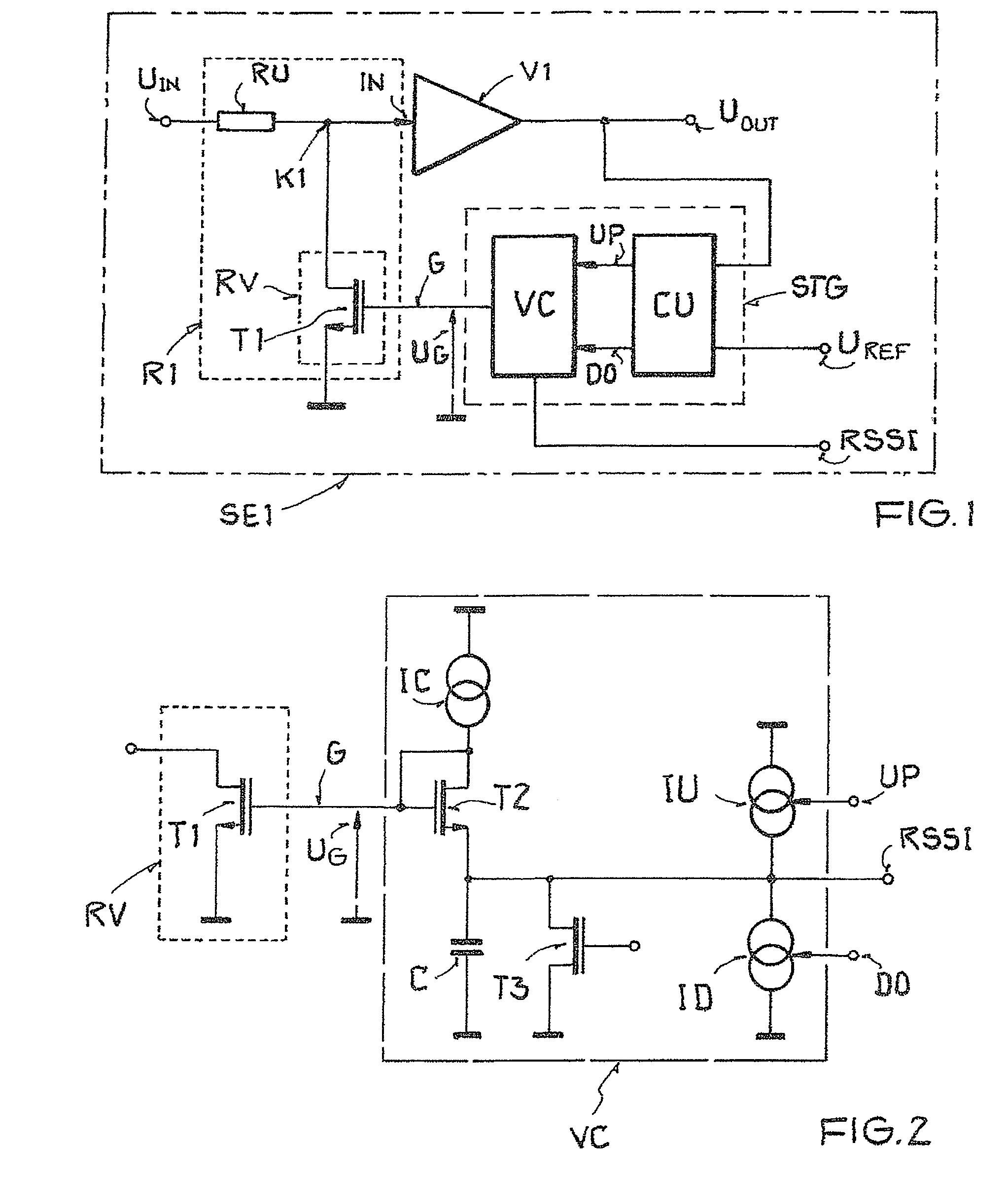
[0021]The task of the receiver unit SE1, shown in FIG. 1, with an internal circuit arrangement is to amplify an input signal UIN, which has an alternating voltage form and is proportional to the field strength of an electromagnetic signal received by a receive antenna (not shown), by means of an operational amplifier V1 by a fixed factor and hereby to hold the output signal UOUT within a predefined interval by means of a control element STG, which changes the resistance value of an input resistance R1, realized as a voltage divider. The circuit arrangement will be described in greater detail below.

[0022]The voltage divider consists of a resistor RU and a MOS transistor T1 linked to a reference potential and realized as a controllable resistance RV. Further, the voltage divider has a node K1, which is connected to the noninverting input of the operational amplifier V1 and to a terminal of MOS transistor T1. Operational amplifier V1 has a fixed amplification factor. The control elemen...


PUM


Abstract

A method for obtaining field strength information from a received electromagnetic signal by a receiver unit, in which an input voltage is generated for an operational amplifier from the received signal in the receiver unit by an input resistance and an output voltage is generated by the operational amplifier by a fixed amplification factor. The input voltage is changed until the output voltage lies within a predefined interval that includes the value of the reference voltage, and hereby the input voltage is tapped at a divider node of a voltage divider and to adjust the output voltage to the reference voltage the gate voltage of the MOS transistor, operating within a nonlinear range, and connected to the divider node is changed in such a way that the forward resistance of the MOS transistor is changed substantially logarithmically and the field strength value received by the receiver unit is determined from a comparison of the value of the present gate voltage with the quantities assigned to the gate voltage values in a memory.

Description

[0001]This nonprovisional application claims priority to German Patent Application No. DE 102009021152.7, which was filed in Germany on May 13, 2009, and to U.S. Provisional Application No. 61 / 177,812, which was filed on May 13, 2009, and which are both herein incorporated by reference.BACKGROUND OF THE INVENTION[0002]1. Field of the Invention[0003]The present invention relates to a method for obtaining field strength information and to a circuit arrangement.[0004]2. Description of the Background Art[0005]A method of this type is known from European Pat. No. EP 1 318 623 B1, which corresponds to U.S. Pat. No. 6,922,553, and which is incorporated herein by reference. Inter alia, a distance between the transmitter and receiver can be determined by means of the field strength information and used for detecting relaying. In general, a so-called “RSSI (Received Signal Strength Indicator)” value, which is proportional to the input signal of a receiving antenna, is determined from the rece...

Claims


Application Information

Patent Timeline
Patent Type & Authority Patents(United States)
IPC IPC(8): H04B17/00
CPCH03F3/193G07C2209/63H03F2200/294
Inventor MOSER, HELMUTMOSER, DANIEL
Owner ATMEL CORP
Why Eureka
Try Eureka