Nonvolatile memory device

a memory device and non-volatile technology, applied in the field of semiconductor devices, can solve the problems of increasing manufacturing costs, difficult to connect and select memory cells in each layer, etc., and achieve the effect of rapid and high-integration

Active Publication Date: 2012-08-21
SAMSUNG ELECTRONICS CO LTD
View PDF7 Cites 5 Cited by
  • Summary
  • Abstract
  • Description
  • Claims
  • Application Information

AI Technical Summary

Benefits of technology

[0007]Example embodiments of inventive concepts provide a nonvolatile memory device that may be more readily and highly integrated into an expanded to a layered structure.

Problems solved by technology

However, it is more difficult to connect and select memory cells in each layer in the nonvolatile memory device having the multilayer structure.
Also, as the number of stacked layers increases, the number of manufacturing operations increases, thereby increasing manufacturing costs.

Method used


Image

  • Nonvolatile memory device
  • Nonvolatile memory device
  • Nonvolatile memory device

Examples


Embodiment Construction

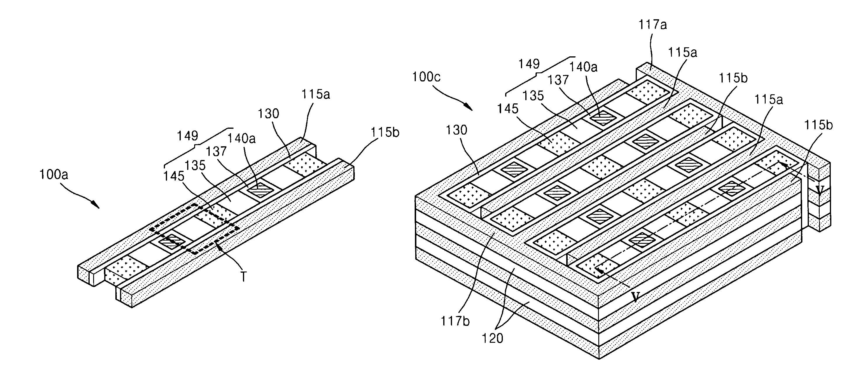
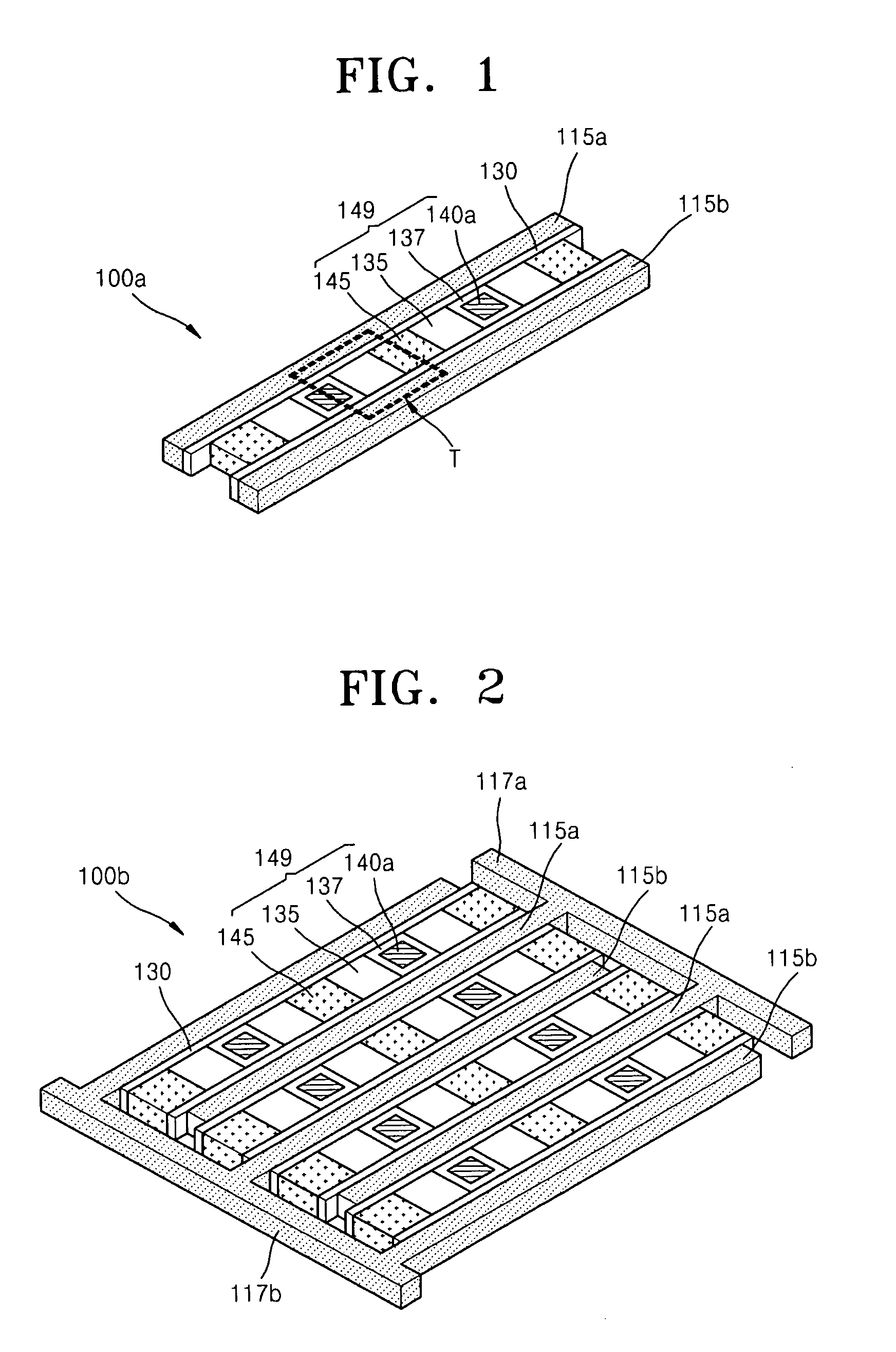
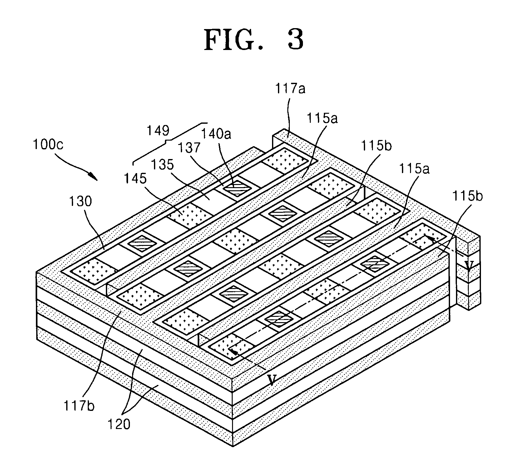
[0024]Hereinafter, the example embodiments will be described in detail with reference to the attached drawings.

[0025]Example embodiments may, however, have many different forms and should not be construed as being limited to those set forth herein; rather, these example embodiments are provided so that this disclosure will be thorough and complete, and will fully convey the concepts of the invention to those of ordinary skill in the art. In the drawings, the sizes and thicknesses of layers and regions are exaggerated for clarity.

[0026]It will be understood that when an element, such as a layer, a region, or a substrate, is referred to as being “on”, “adjacent to”, “connected to”, or “coupled to” another element, it may be directly on, adjacent to, connected to, or coupled to the other element or intervening elements may be present. In contrast, when an element is referred to as being “directly on”, “directly connected to” or “directly coupled to” another element, there are no interv...


PUM


Abstract

The nonvolatile memory device includes at least one pair of first electrode lines, at least one device structure disposed between the at least one pair of first electrode lines and a dielectric layer disposed between the at least one device structure and the at least one pair of first electrode lines. The at least one device structure includes a second electrode line including a first conductive type semiconductor, a resistance changing material layer adjacent to the second electrode line, a channel adjacent to the resistance changing material layer and including a second conductive type semiconductor different from the first conductive type semiconductor and a third electrode line adjacent to the channel and including the first conductive type semiconductor.

Description

CROSS-REFERENCE TO RELATED APPLICATION(S)[0001]This application claims the benefit of Korean Patent Application No. 10-2009-0023543, filed on Mar. 19, 2009, in the Korean Intellectual Property Office, the disclosure of which is incorporated herein in its entirety by reference.BACKGROUND[0002]1. Field[0003]Example embodiments of inventive concepts relate to a semiconductor device, for example, to a nonvolatile memory device using a resistance changing material layer.[0004]2. Description of the Related Art[0005]A volume of a semiconductor product is continuously decreasing, while the semiconductor product is still required to process a high capacity of data. Accordingly, an operation speed and integration of a nonvolatile memory device used in such a semiconductor product needs to be increased. Here, a nonvolatile memory device having a multilayer structure is more highly integrated than a nonvolatile memory device having a conventional monolayer structure.[0006]By using the multilaye...

Claims


Application Information

Patent Timeline
Patent Type & Authority Patents(United States)
IPC IPC(8): H01L45/00
CPCH01L27/2436H01L27/2445H01L27/249H01L45/06H01L45/1226H01L45/144H01L45/146H01L45/147H10B63/32H10B63/845H10B63/30H10N70/823H10N70/20H10N70/8836H10N70/231H10N70/8828H10N70/8833H10N70/8825
Inventor SEOL, KWANG-SOOPARK, YOON-DONGKIM, DEOK-KEECHOI, SANG-JUN
Owner SAMSUNG ELECTRONICS CO LTD
Why Eureka
Try Eureka