Method of driving organic electroluminescence emission portion

a technology of electroluminescence and emission portion, which is applied in the direction of instruments, computing, electric digital data processing, etc., can solve the problem of worsening the uniformity of the luminance of the image displayed, and achieve the effect of shortening the tim

Active Publication Date: 2012-08-21
JOLED INC
View PDF14 Cites 2 Cited by
  • Summary
  • Abstract
  • Description
  • Claims
  • Application Information

AI Technical Summary

Benefits of technology

[0028]In the light of the foregoing, it is therefore desirable to provide a method, of driving an organic electroluminescence emission portion, which is capable of ensuring long a time allocated to threshold voltage canceling processing, and executing the threshold voltage canceling processing and the like with no difficulty.
[0050]In the driving method according to the embodiment of the present invention, for the predetermined scanning time period, the first node initialization voltage is applied to the corresponding one of the drive lines, and next, the video signal is supplied instead of applying the first node initialization voltage. Also, as described above, the write transistor is turned ON prior to the commencement of the scanning time period for which the step (a) is intended to be performed in accordance with a signal from the corresponding one of the scanning lines, and the step (a) is then performed. As a result, the potential at the first node is initialized as soon as the first node initialization voltage is applied to the corresponding one of the data lines. In the configuration for turning ON the write transistor after the voltage applied to the corresponding one of the data lines is switched over to the first node initialization voltage, a time, including a time for waiting for the switching, needs to be allocated to the processing. On the other hand, in the driving method according to the embodiment of the present invention, a time for waiting for the switching is unnecessary, and thus the preprocessing can be executed for a shorter time. As a result, a longer time can be allocated to the threshold voltage canceling processing which is executed next to the preprocessing.
[0054]The drive voltage described above, and the voltage applied to one of the source / drain regions of the drive transistor in the step (b) may be different from each other. However, preferably, the power source portion applies the drive voltage to one of the source / drain regions of the drive transistor in the step (b) and the step (d) from a viewpoint of reducing the kinds of voltages each of which is supplied from the power source portion.
[0056]Although the details of the drive circuit will be described later, the drive circuit concerned can be configured in the form of a drive circuit composed of two transistors and one capacitor portion (called a 2Tr / 1C drive circuit), three transistors and one capacitor portion (called a 3Tr / 1C drive circuit) or four transistors and one capacitor portion (called a 4Tr / 1C drive circuit). In any of the drive circuits, the number of transistors is reduced as compared with the drive circuit shown in FIG. 19, and thus the configuration of the drive circuit is simplified.
[0069]According to the driving method of the present invention, the first node initialization voltage is applied to the corresponding one of the drive lines for the predetermined scanning time period, and next, the video signal is supplied instead of applying the first node initialization voltage. Also, as described above, the write transistor is turned ON prior to the commencement of the scanning time period for which the step (a) is intended to be performed in accordance with a signal from the corresponding one of the scanning lines, and the step (a) is then performed. As a result, the potential at the first node is initialized as soon as the first node initialization voltage is applied to the corresponding one of the data lines. In the constitution for turning ON the write transistor after the voltage applied to the corresponding one of the data lines is switched over to the first node initialization voltage, a time, including a time for waiting for the switching, needs to be allocated to the processing. On the other hand, in the driving method according to the embodiment of the present invention, a time for waiting for the switching is unnecessary, and thus the preprocessing can be executed for a shorter time. As a result, a longer time can be allocated to the threshold voltage canceling processing which is executed next to the preprocessing.

Problems solved by technology

In particular, when the time allocated to the threshold voltage canceling processing becomes shorter, the correction for the dispersion of the characteristics of the drive transistor becomes insufficient, so that the uniformity of the luminance of the image displayed becomes worse.

Method used


Image

  • Method of driving organic electroluminescence emission portion
  • Method of driving organic electroluminescence emission portion
  • Method of driving organic electroluminescence emission portion

Examples


embodiment 1

[0127]Embodiment 1 relates to a method of driving the organic electroluminescence emission portion of the present invention. In Embodiment 1, the drive circuit is configured in the form of a 2Tr / 1C drive circuit.

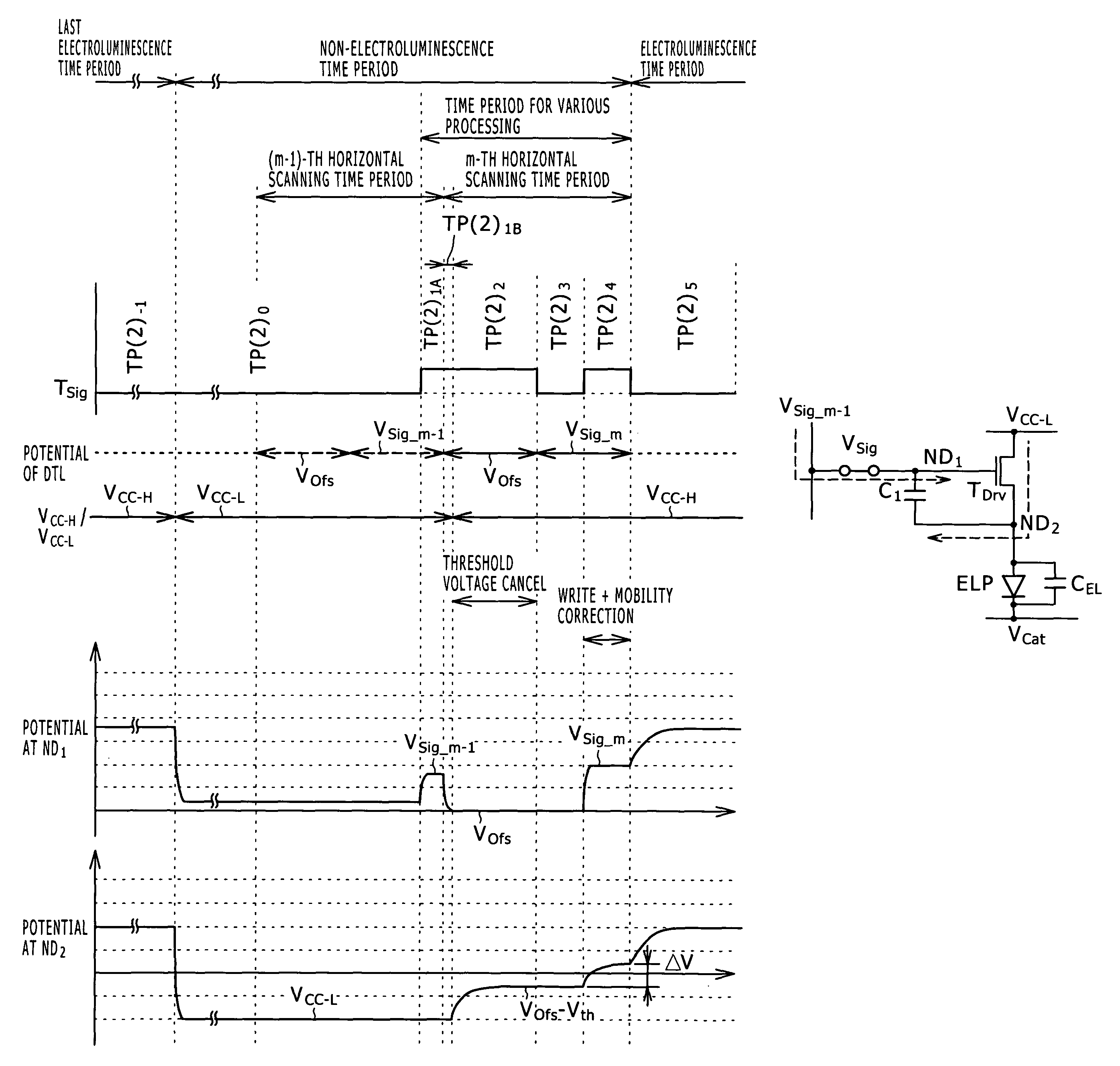
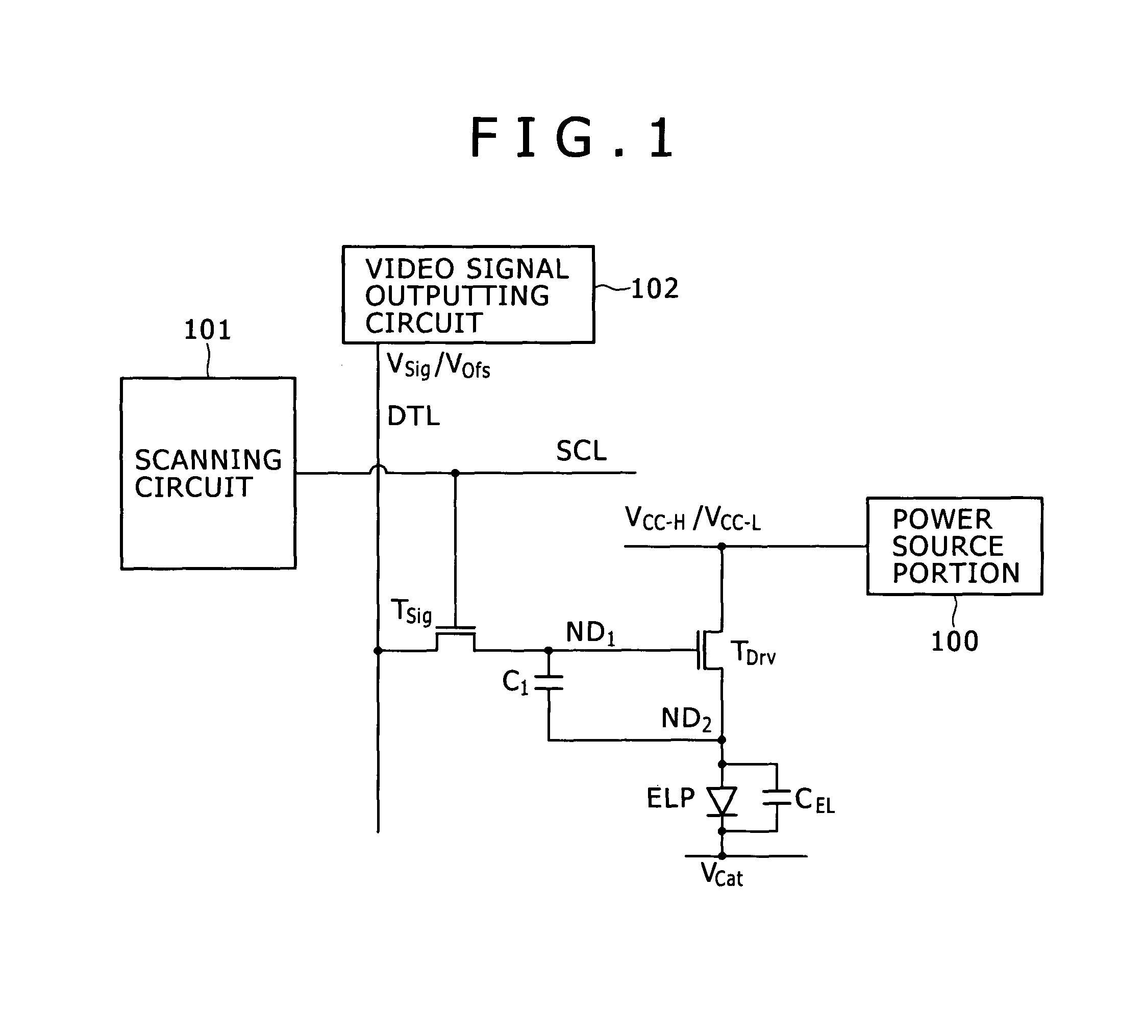
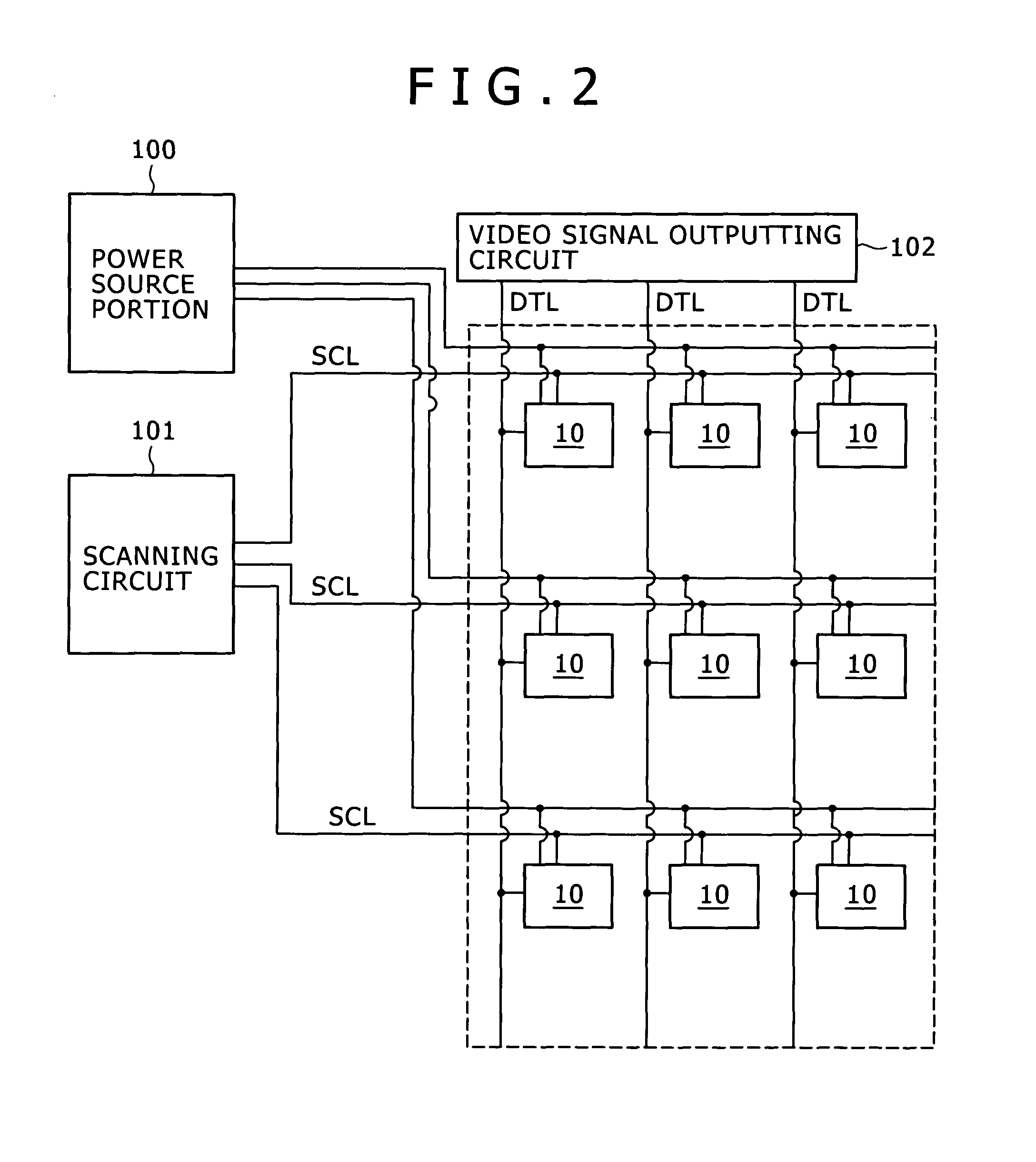
[0128]FIG. 1 shows an equivalent circuit diagram of the 2Tr / 1C drive circuit, and FIG. 2 shows a conceptual view of the organic EL display device. Also, FIG. 4 schematically shows a timing chart in a drive operation, FIGS. 5A to 5I schematically show an ON / OFF state and the like of the transistors, and FIG. 6 shows a timing chart in the drive operation in a comparative example.

[0129]The 2Tr / 1C drive circuit is composed of the two transistors of the write transistor TSig and the drive transistor TDrv, and one capacitor portion C1.

[Drive Transistor TDrv]

[0130]As described above, one of the source / drain regions of the drive transistor TDrv is connected to the power source portion 100. On the other hand, the other of the source / drain regions of the drive transistor TDrv is conne...

embodiment 2

[0193]Embodiment 2 is a change of Embodiment 1. In Embodiment 1, the operation from the step (a) to the step (c) is performed for the m-th horizontal scanning time period. Embodiment 2 is principally different from Embodiment 1 in that the operation from the step (a) to the step (c) is performed for a plurality of horizontal scanning time periods.

[0194]Since the configurations of the organic EL display device and the drive circuit in Embodiment 2 are the same as those of the organic EL display device and the drive circuit in Embodiment 1, a description thereof is omitted here for the sake of simplicity. FIG. 7 schematically shows a timing chart in a drive operation in Embodiment 2, and FIGS. 8A to 8I schematically show an ON / OFF state and the like of the drive transistor and the write transistor.

[0195]As has been described above, in Embodiment 2, the operation from the step (a) to the step (c) is performed for a plurality of scanning time periods. Hereinafter, a description will be ...

embodiment 3

[0224]Embodiment 3 also relates to a method of driving an organic electroluminescence (EL) portion of the present invention. In Embodiment 3, the drive circuit is configured in the form of a 4Tr / 1C drive circuit.

[0225]FIG. 9 shows an equivalent circuit diagram of the 4Tr / 1C drive circuit, and FIG. 10 shows a conceptual view of an organic EL display device. Also, FIG. 11 schematically shows a timing chart in a drive operation, and FIGS. 12A to 12J schematically show an ON / OFF state and the like of the four transistors.

[0226]The 4Tr / 1C drive circuit also includes two transistors of the write transistor TSig and the drive transistor TDrv, and one capacitor portion C1 similarly to the case of the 2Tr / 1C drive circuit described above. Also, the 4Tr / 1C drive circuit further includes an electroluminescence controlling transistor TEL—C, and a second node initializing transistor TND2.

[0227]The electroluminescence controlling transistor TEL—C is composed of an n-channel TFT including source / d...


PUM


Abstract

Disclosed herein is a method of driving an organic electroluminescence emission portion, the method including the steps of: applying a first node initialization voltage to corresponding one of the data lines, and supplying the video signal instead of the first node initialization voltage for a predetermined scanning time period, applying the first node initialization voltage from the corresponding one of the data lines to the first node through the write transistor held in an ON state for initializing the potential at the first node, and holding a state of applying the first node initialization voltage from the corresponding one of the data lines to the first node through the write transistor held in an ON state for holding the potential at the first node.

Description

CROSS REFERENCES TO RELATED APPLICATIONS[0001]The present invention contains subject matter related to Japanese Patent Application JP 2007-230047 filed in the Japan Patent Office on Sep. 5, 2007, the entire contents of which being incorporated herein by reference.BACKGROUND OF THE INVENTION[0002]1. Field of the Invention[0003]The present invention relates to methods of driving an organic electroluminescence emission portion.[0004]2. Description of the Related Art[0005]In an organic electroluminescence display device (hereinafter simply referred to as “an organic EL display device” for short when applicable) using an organic electroluminescence element (hereinafter simply referred to as “an organic EL element” for short when applicable) as an electroluminescence element, a luminance of the organic EL element is controlled in accordance with a value of a current caused to flow through the organic EL element. Also, a simple matrix system and an active matrix system are well known as a ...

Claims


Application Information

Patent Timeline
Patent Type & Authority Patents(United States)
IPC IPC(8): G09G3/30
CPCG09G3/3233G09G3/3291G09G2300/0417G09G2310/0251G09G2300/0842G09G2300/0861G09G2300/0819
Inventor TOYOMURA, NAOBUMIYAMAMOTO, TETSUROUCHINO, KATSUHIDE
Owner JOLED INC
Why Eureka
Try Eureka