Method of manufacturing strained-silicon semiconductor device

a technology of strained silicon and semiconductors, applied in the direction of individual semiconductor device testing, semiconductor/solid-state device testing/measurement, instruments, etc., can solve the problems of lack of planarity when seg is performed, small components are now so small, etc., and achieve the effect of increasing the local epitaxial concentration ratio percentag

Active Publication Date: 2012-08-28
TAIWAN SEMICON MFG CO LTD
View PDF14 Cites 93 Cited by
  • Summary
  • Abstract
  • Description
  • Claims
  • Application Information

AI Technical Summary

Problems solved by technology

Components are now so small, however, that advances in speed are not necessarily resulting simply from reductions in size.
One problem with using the selective epitaxial growth (SEG) strained-silicon approach is local loading.
This tends to cause a lack of planarity when SEG is performed, a significantly undesirable condition.
These types of voids could degrade device performance, and could also serve as the defect source in subsequent process steps.

Method used


Image

  • Method of manufacturing strained-silicon semiconductor device
  • Method of manufacturing strained-silicon semiconductor device
  • Method of manufacturing strained-silicon semiconductor device

Examples


Embodiment Construction

[0030]The making and using of the presently preferred embodiments are discussed in detail below. It should be appreciated, however, that the present invention provides many applicable inventive concepts that can be embodied in a wide variety of specific contexts. The specific embodiments discussed are merely illustrative of specific ways to make and use the invention, and do not limit the scope of the invention. The present invention will be described with respect to preferred embodiments in a specific context, namely a semiconductor device consisting of a substrate populated with a plurality of substantially identical transistors. The invention may also be applied, however, to other semiconductor devices as well.

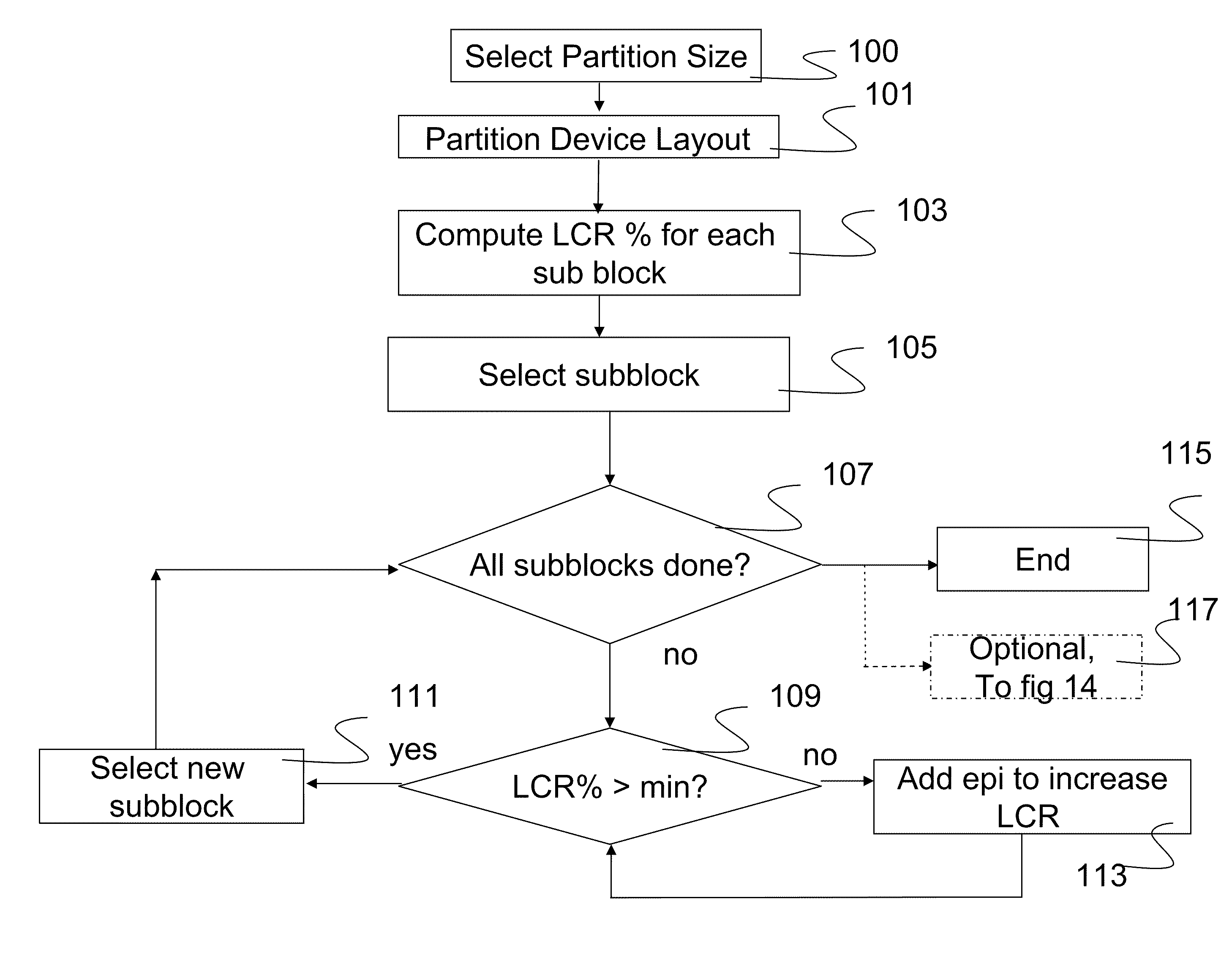
[0031]The present invention involves a method of manufacturing semiconductor devices. Specifically, the present invention is directed at a method of implementing selective epitaxial growth (SEG) with reduced local-loading effects in order to produce a more uniform epitaxial...


PUM


Abstract

A method for fabricating a strained-silicon semiconductor device to ameliorate undesirable variation in selectively grown epitaxial film thickness. The layout or component configuration for the proposed semiconductor device is evaluated to determine areas of relatively light or dense population in order to determine whether local-loading-effect defects are likely to occur. If a possibility of such defects occurring exists, a dummy pattern of epitaxial structures may be indicated. If so, the dummy pattern appropriate to the proposed layout is created, incorporated into the mask design, and then implemented on the substrate along with the originally-proposed component configuration.

Description

[0001]This application is a continuation in part of U.S. patent application Ser. No. 11 / 272,938, filed Nov. 14, 2005, and entitled “Method of Manufacturing Strained-Silicon Semiconductor Device,” which application is hereby incorporated herein by reference.TECHNICAL FIELD[0002]The present invention relates generally to a method for fabricating semiconductors, and more particularly to a method for fabricating a semiconductor device to reduce the undesirable effects of local loading while employing selective epitaxial growth (SEG) in a strained silicon fabrication.BACKGROUND[0003]Electronic devices using semiconductors are utilized in a wide variety of applications. They provide the computing capability and data storage that make possible not only the operation of computers, large and small, but also things like electronic gaming devices, home entertainment systems, and telephones and other communications equipment. Advances in technology have made possible not only the construction o...

Claims


Application Information

Patent Timeline
Patent Type & Authority Patents(United States)
IPC IPC(8): G06F17/50
CPCH01L21/823807H01L21/823814H01L27/0207H01L29/7848
Inventor CHEN, YUN-HSIUJANG, SYUN-MINGTSAI, PANG-YEN
Owner TAIWAN SEMICON MFG CO LTD
Why Eureka
Try Eureka