

Solver for modeling a multilayered integrated circuit with three-dimensional interconnects
a multi-layer integrated circuit and solver technology, applied in the field of multi-layer circuit design, can solve the problems of limited analysis of the effects of each circuit layer, inadequate conventional modeling of the layers, etc., and achieve the effect of improving computational efficiency
- Summary
- Abstract
- Description
- Claims
- Application Information
AI Technical Summary
Benefits of technology
Problems solved by technology
Method used
Image

Examples
Embodiment Construction
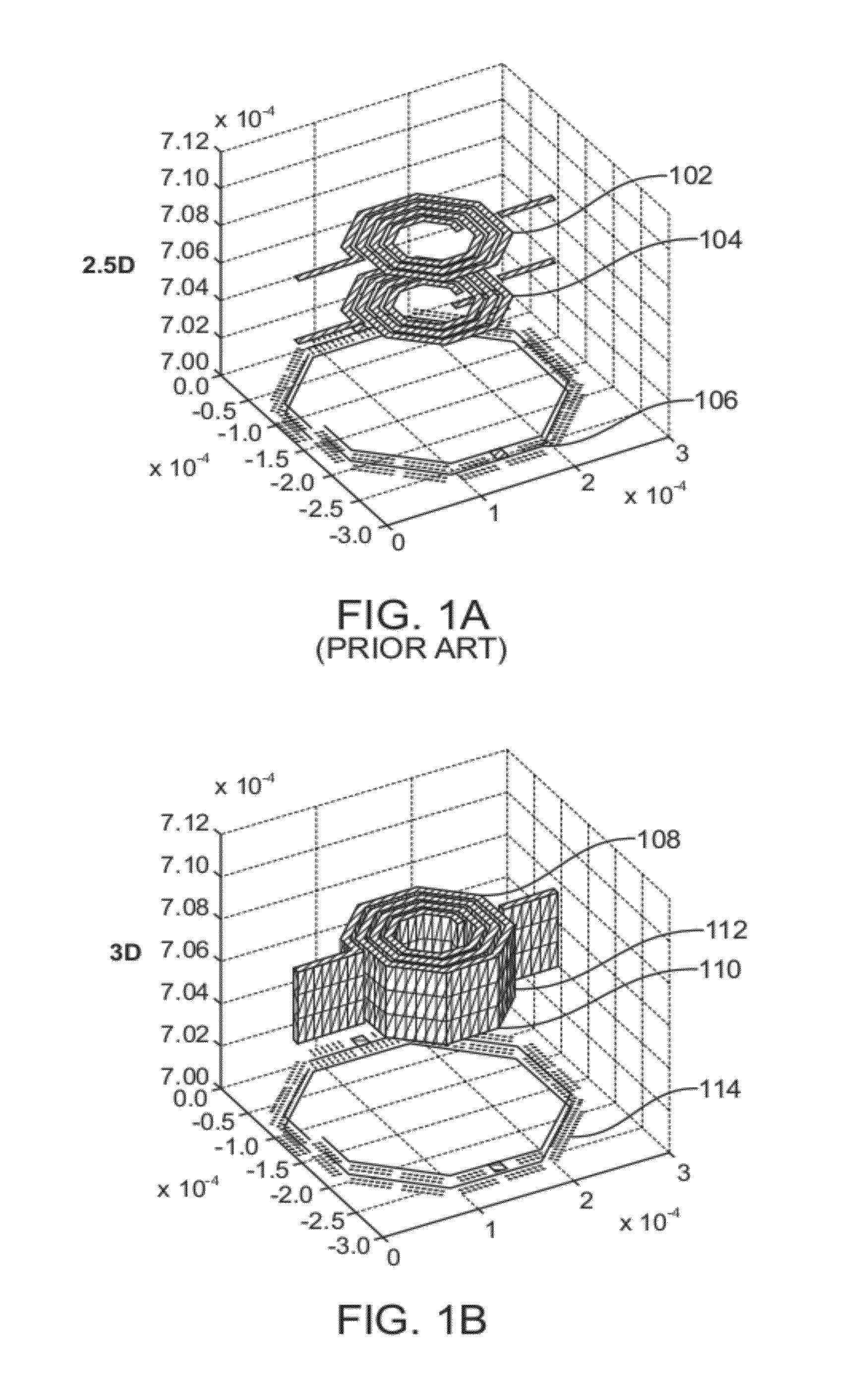
[0046]FIG. 1A shows a conventional “2.5D model” (i.e., 2.5 dimensional) of a spiral inductor with a mesh model for a top wall 102 and a bottom wall 104. A lower layer 106 on the substrate is also shown. The 2.5D model supports current flow in the x-direction and y-direction only while implicitly introducing z-directed currents (i.e., normal to the substrate) in association with the via currents. See, for example, “Method and apparatus for determining interactive electromagnetic effects among conductors of a multi-layer circuit”, U.S. Pat. No. 7,127,688, issued Oct. 24, 2006, which is incorporated by reference in its entirety. See also “Large-scale Broadband Parasitic Extraction for Fast Layout Verification of 3-D RF and Mixed-Signals On-chip Structures”, F. Ling et al., IEEE Transactions on Microwave Theory and Techniques, Vol. 53, No. 1, January 2005.
[0047]In general, the 2.5D model has provided sufficient accuracy in when the layout conductors are predominantly thin. In today's 90...
PUM
 Abstract
Description
Claims
Application Information