Lead frame and intermediate product of semiconductor device

a technology of semiconductor devices and intermediate products, which is applied in the direction of semiconductor devices, semiconductor/solid-state device details, electrical devices, etc., can solve the problems of resin peeling on the outer frame, and achieve the effect of facilitating reducing the occurrence of defective parts of the intermediate product of the semiconductor devi

a technology of semiconductor devices and intermediate products, which is applied in the direction of semiconductor devices, semiconductor/solid-state device details, electrical devices, etc., can solve the problems of resin peeling on the outer frame, and achieve the effect of facilitating reducing the occurrence of defective parts of the intermediate product of the semiconductor devi

US8258608B2Active Publication Date: 2012-09-04ADVANCED SEMICON ENG INC

Image

  • Lead frame and intermediate product of semiconductor device
  • Lead frame and intermediate product of semiconductor device
  • Lead frame and intermediate product of semiconductor device

Examples


Embodiment Construction

[0041]Subsequently, an embodiment for embodying the invention will be described with reference to the accompanying drawings, and serves for understanding of the invention.

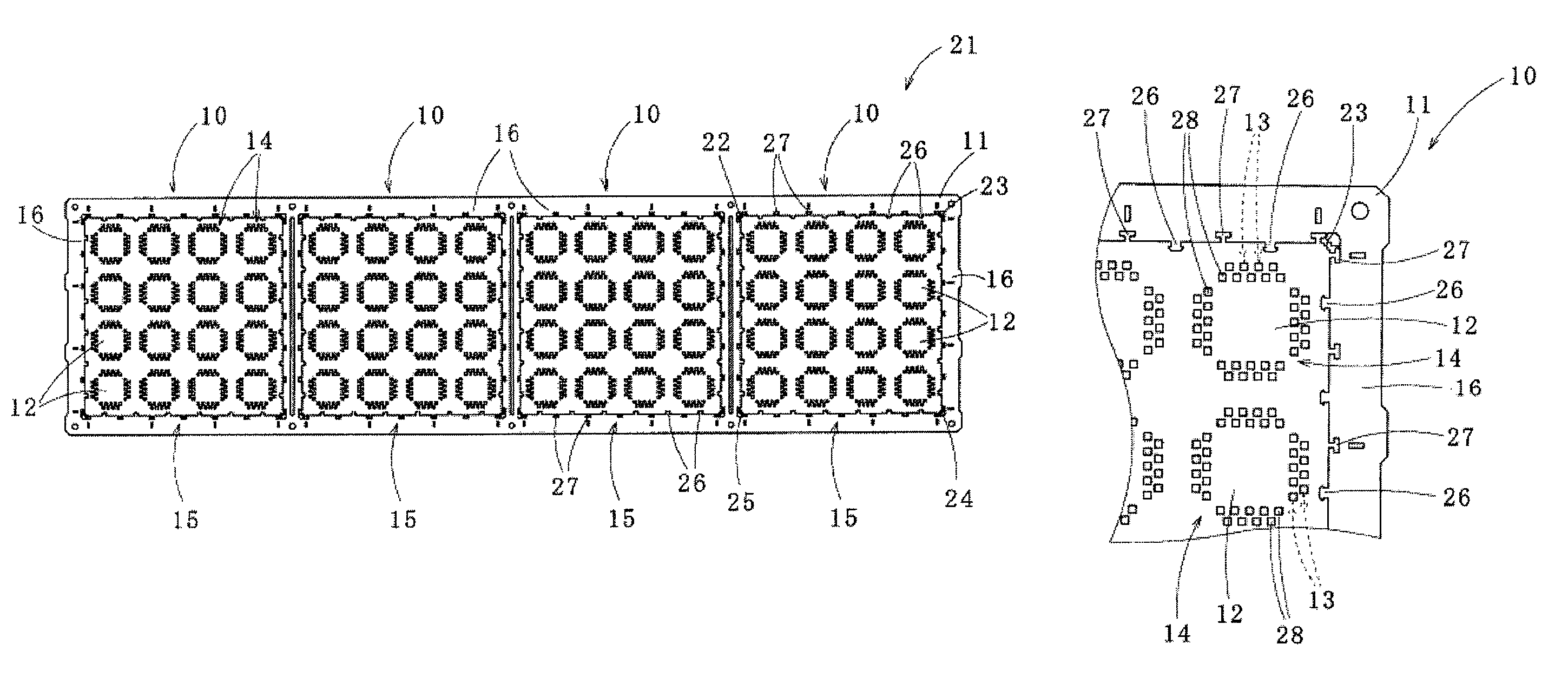
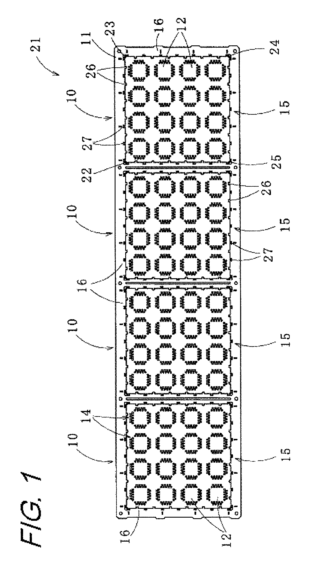
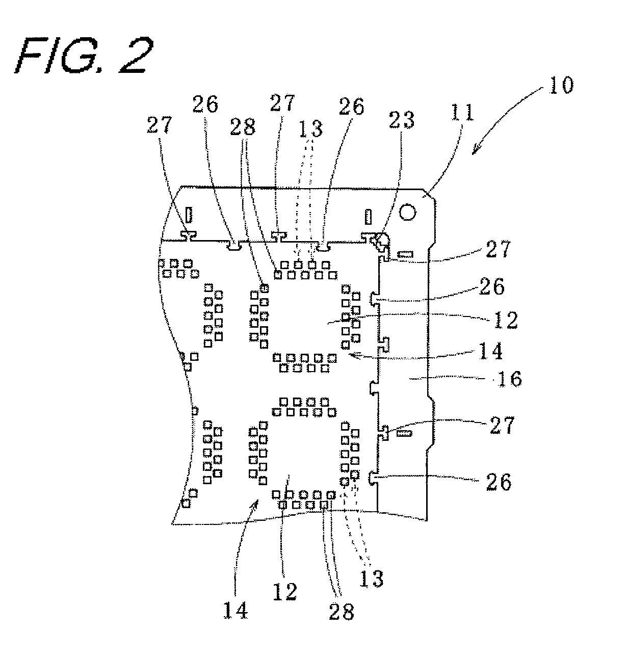
[0042]As shown in FIGS. 1, 2 and 6A to 6C, a lead frame 10 according to one embodiment of the invention is used for manufacturing a semiconductor device 20 by forming a circuit pattern group 15 including unit lead frames 14 having plural upper side terminal parts 13 in the periphery of a semiconductor element mounting region 12 in plural lines by the first etching and an outer frame 16 surrounding the circuit pattern group 15 in a state of having a gap in a lead frame material 11 made of copper or copper alloy and then mounting a semiconductor element 17 every the unit lead frame 14 and carrying out necessary wiring and further enclosing the entire surface of the circuit pattern group 15 in which the semiconductor element 17 is mounted and a part of the outer frame 16 with a resin 18 from an upper surface side and ...


PUM


Abstract

In a lead frame used for manufacturing a semiconductor device by forming a circuit pattern group including unit lead frames having plural upper side terminal parts in the periphery of a semiconductor element mounting region in one line or plural lines and an outer frame surrounding the circuit pattern group in a state of having a gap in a lead frame material and then mounting a semiconductor element every the unit lead frame and carrying out necessary wiring and enclosing the entire surface of the circuit pattern group in which the semiconductor element is mounted and a part of the outer frame with a resin from an upper surface side and further etching from a lower surface side and forming lower side terminal parts joined to the upper side terminal parts of the circuit pattern group, the circuit pattern group and the outer frame are had and the inner edge of the outer frame is formed in an uneven portion in plan view and bonding between the resin and the outer frame is enhanced.

Description

BACKGROUND OF THE INVENTION[0001]1. Field of the Invention[0002]The present invention relates to a lead frame used in manufacture of a semiconductor device, and an intermediate product of the semiconductor device using its lead frame.[0003]2. Related Art[0004]In manufacture of a semiconductor device, a reduction in manufacturing cost is desired, and a method for manufacturing the semiconductor device at low cost without using resin tape, adhesive tape, etc. is proposed in, for example, JP-A-2001-24135.[0005]In the manufacturing method of the semiconductor device of JP-A-2001-24135, a noble metal plated layer is first formed on an external connection terminal part of a lower surface side, a portion or all of an outer frame and a wire bonding part of an upper surface side of a lead frame material, and half etching processing of the upper surface side of a lead frame material is performed. Next, after a semiconductor element is mounted, wire bonding is performed and the upper surface s...

Claims


Application Information

Patent Timeline
04 Sep 2012
Publication
US8258608B2
IPC
H01L21/02
CPC
H01L21/4832; H01L23/49541; H01L24/48; H01L24/49; H01L24/97; H01L2924/01005; H01L2224/48091; H01L2224/48247
Inventors
TAKAI, KEIJI