
Implantable lead for an active medical device having an inductor design minimizing eddy current losses

a technology of inductance and lead, applied in the direction of inductance, impedence network, therapy, etc., to achieve the effect of low resistive loss, high equivalent series resistance, and low resistance loss

Active Publication Date: 2012-09-04
WILSON GREATBATCH LTD
View PDF16 Cites 19 Cited by
  • Summary
  • Abstract
  • Description
  • Claims
  • Application Information

AI Technical Summary

Benefits of technology

The present invention provides a shielded component or network for an active medical device (AMD) implantable lead that minimizes eddy current losses in the implantable housing. The invention includes an inductor and a capacitor, with the inductor having a primary magnetic field line axis oriented perpendicular to the length of the lead. The conductive shield or housing surrounds the lead and includes a primary longitudinal axis. The use of an inductor design reduces eddy current losses in the implantable housing. The inductor may be a solenoid inductor, chip inductor, or a thick film inductor. The capacitor may be a chip capacitor or a feedthrough capacitor. The inductor and capacitor may be electrically connected in parallel to form a bandstop filter, which is tuned to impede induced current flow through the lead at a selected center frequency or range of frequencies. The bandstop filter is designed to minimize the impact of parasitic effects caused by the metallic tube housing. The invention also includes a non-conductive insulator or dielectric material between the passive component network and the conductive shield or housing. The invention provides a more effective solution for minimizing eddy current losses in the implantable lead.

Problems solved by technology

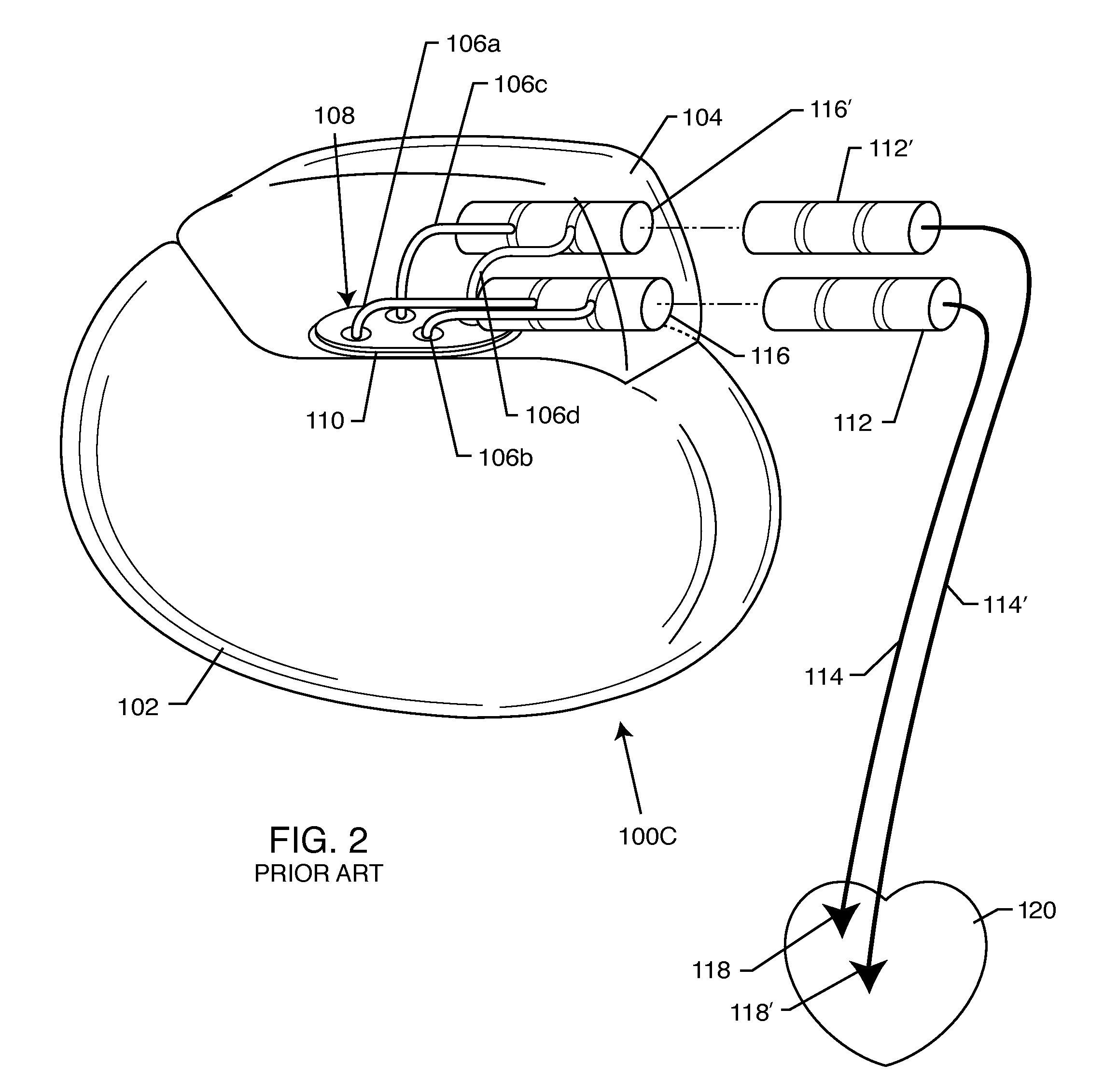
However, the use of a metallic tube to create the outer housing creates challenges to minimize parasitic effects on the inductor utilized in the circuit design.

Method used


Image

  • Implantable lead for an active medical device having an inductor design minimizing eddy current losses
  • Implantable lead for an active medical device having an inductor design minimizing eddy current losses
  • Implantable lead for an active medical device having an inductor design minimizing eddy current losses

Examples


Embodiment Construction

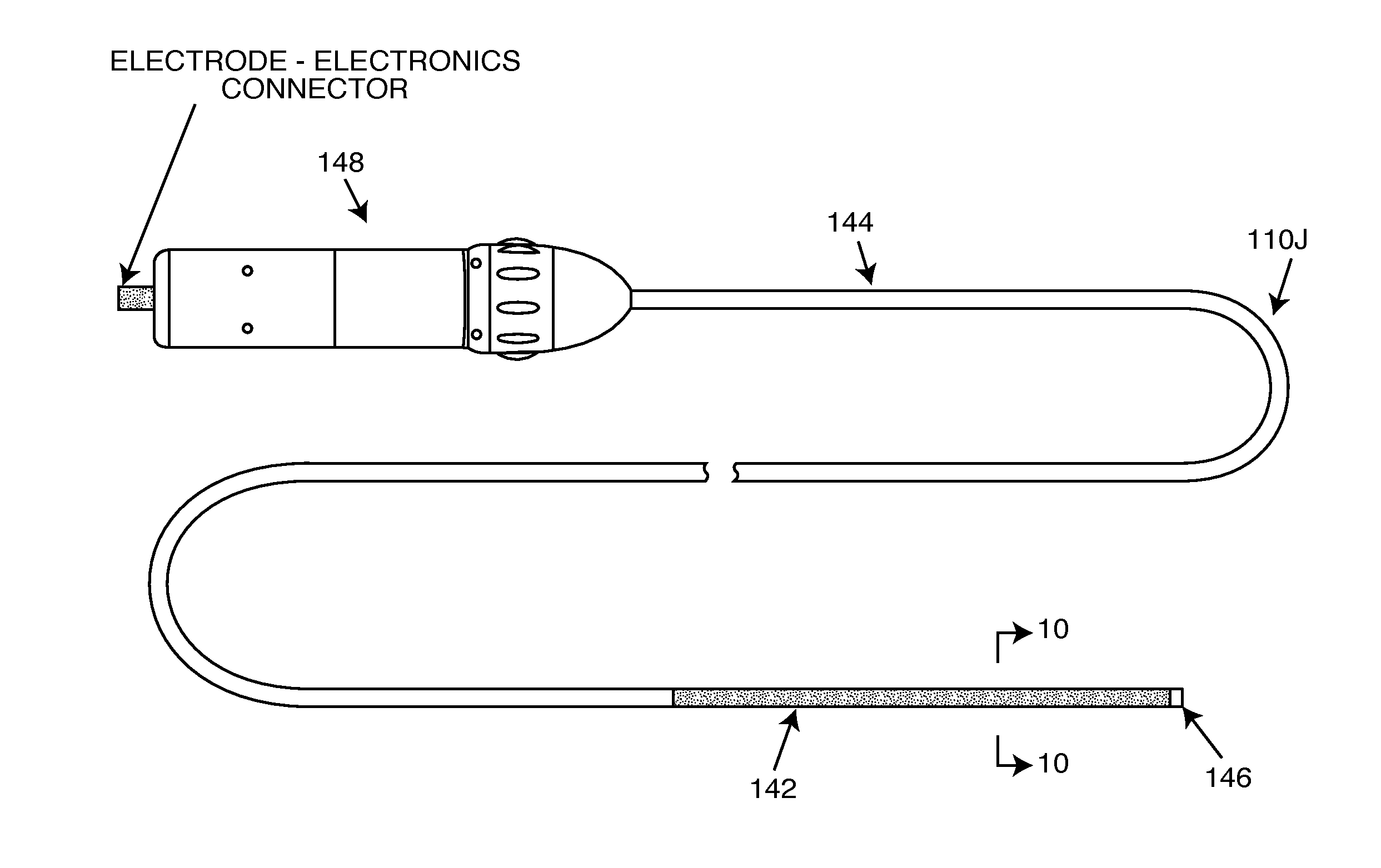
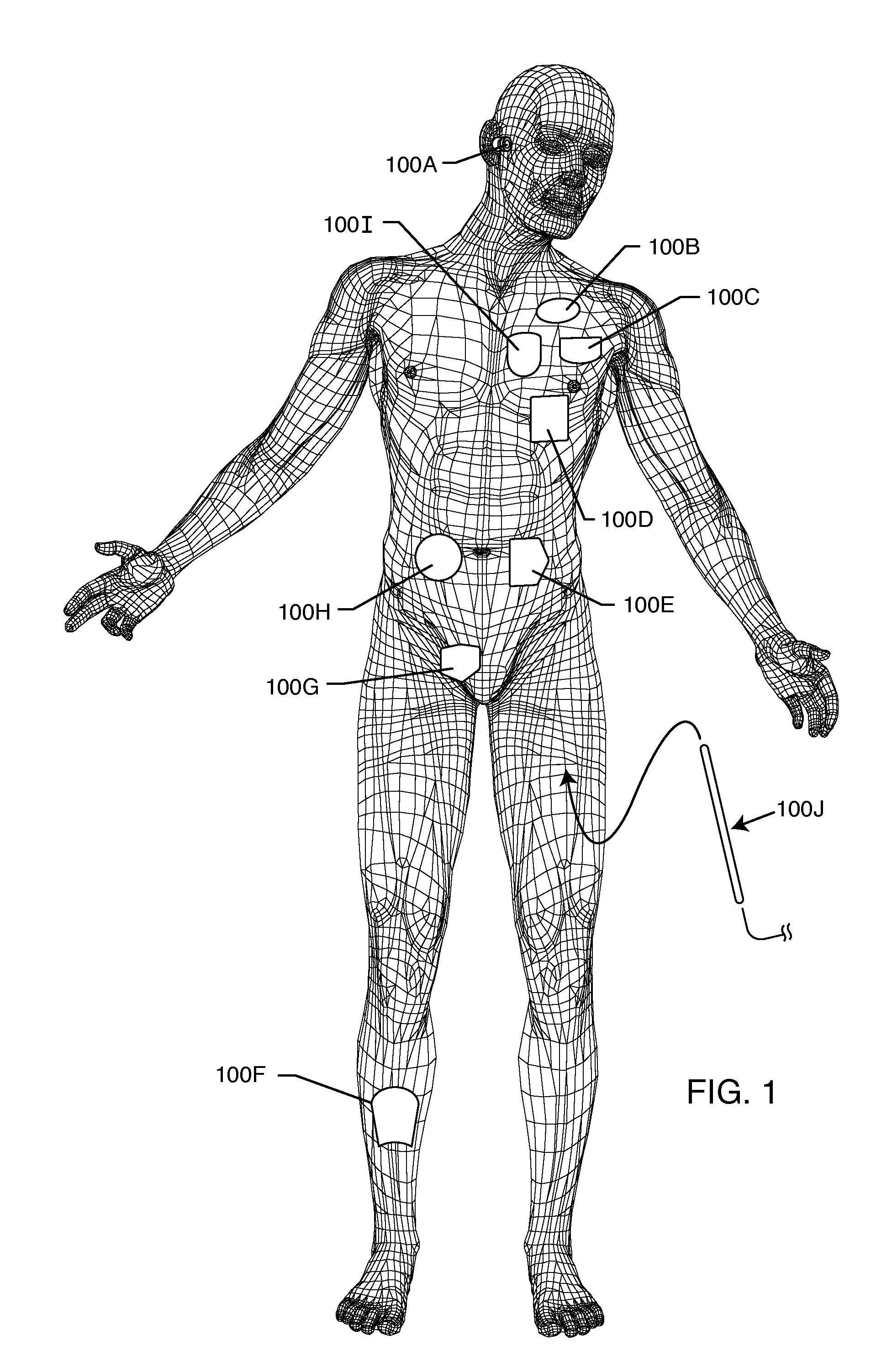
[0113]As shown in the drawings for purposes of illustration, the present invention relates to a system for RF shielding of a passive component or network disposed along the length of implanted leads of active medical devices (AMDs). In particular, the conductive RF shielding is to shield and / or hermetically seal a passive inductor or inductive component in the presence of high power electromagnetic field environments, such as the RF pulsed fields produced by a clinical MRI scanner. In a broad sense, the present invention comprises an active medical device system including an implanted lead having RE shielded inductors or passive network components including inductors. The implanted lead may be coaxial, rectangular, flat or other geometries. US 2009 / 0243756 is incorporated herein by reference. Furthermore, the implanted lead may consist of a number of internal conductors, such as a bipolar lead for cardiac pacemaker channel or even an eight or sixteen conductor spinal cord stimulator...


PUM


Abstract

A shielded component or network for an active medical device (AMD) implantable lead includes an implantable lead having a length extending from a proximal end to a distal end, all external of an AMD housing, and a passive component or network disposed somewhere along the length of the implantable lead. The passive component or network including at least one inductive component having a primary magnetic field line axis. A conductive shield or housing having a primary longitudinal axis substantially surrounds the inductive component or the passive network. The inductive component's magnetic field line axis is oriented substantially orthogonally to the primary longitudinal axis of the conductive shield or housing.

Description

FIELD OF THE INVENTION[0001]This invention generally relates to the problem of high frequency energy induced onto implanted leads during medical diagnostic procedures such as magnetic resonant imaging (MRI). More specifically, the present invention relates to an implantable medical system comprised of an active medical device (AMD) and at least one lead extending exteriorly from a proximal end at or adjacent to the AMD, to a biological sensing or stimulating electrode at a distal end. The lead has a passive component or network including at least one inductive component disposed somewhere along its length between the proximal end and distal end. The inductive component has a primary magnetic field line axis, and is substantially surrounded by a conductive shield or housing that itself has a primary longitudinal axis oriented substantially orthogonally to the inductive component's magnetic field line axis. Such a lead-based inductor design minimizes eddy current losses.BACKGROUND OF ...

Claims


Application Information

Patent Timeline
Patent Type & Authority Patents(United States)
IPC IPC(8): A61N1/00
CPCA61N1/05H01F17/00H01F27/36H03H1/0007H03H7/0115A61N1/3718A61N2001/086H03H2001/0042H03H2007/013A61N1/086H01F27/363H01F27/366
Inventor JOHNSON, ROBERT SHAWNDABNEY, WARREN S.MOSCHIANO, HOLLY NOELLESTEVENSON, ROBERT A.
Owner WILSON GREATBATCH LTD
Learn More