Semiconductor device and method of manufacturing thereof

a semiconductor and semiconductor technology, applied in semiconductor devices, semiconductor/solid-state device details, electrical devices, etc., can solve the problems of forming voids, difficult to accurately control sealing-resin coatings, and breakage of wires and contact between wires, so as to reduce warping of semiconductor chips and printed circuit boards, reduce manufacturing costs, and improve sealing

Active Publication Date: 2012-09-11
DOW TORAY CO LTD
View PDF9 Cites 16 Cited by
  • Summary
  • Abstract
  • Description
  • Claims
  • Application Information

AI Technical Summary

Benefits of technology

[0008]It is an object of the present invention to provide a method for efficient manufacturing of sealed semiconductor devices that prevent formation of voids in the sealing material and reduce warping of semiconductor chips and printed-circuit boards, which in case of sealing with a curable liquid silicone composition, can be sealed quickly and with adequate moldability. It is another object to provide sealed semiconductor devices with the aforementioned properties.

Problems solved by technology

If a transfer-molding is employed in resin sealing of thin packages, the thickness of the sealing resin could be precisely controlled, whereas there are problems that vertical displacements of semiconductor chips occur in a flow of a liquid sealing resin, or breakage of wires and contact between the wires occur because of deformations of bonding wires connected to semiconductor chips under the effect of pressure in the flow of the liquid sealing resin.
On the other hand, although potting or screen-printing with a liquid sealing resin to some extent protects the bonding wires from breakage and mutual contact, these methods make accurate control of sealing-resin coatings more difficult and can easily lead to formation of voids.
However, due to thinning of semiconductor chips that occurs with miniaturization of semiconductor elements, these methods increase warping of the semiconductor chips and printed-circuit boards and may lead to damaging of semiconductor devices and to worsening of their performance characteristics.

Method used


Image

  • Semiconductor device and method of manufacturing thereof
  • Semiconductor device and method of manufacturing thereof
  • Semiconductor device and method of manufacturing thereof

Examples


example 1

Practical Example 1

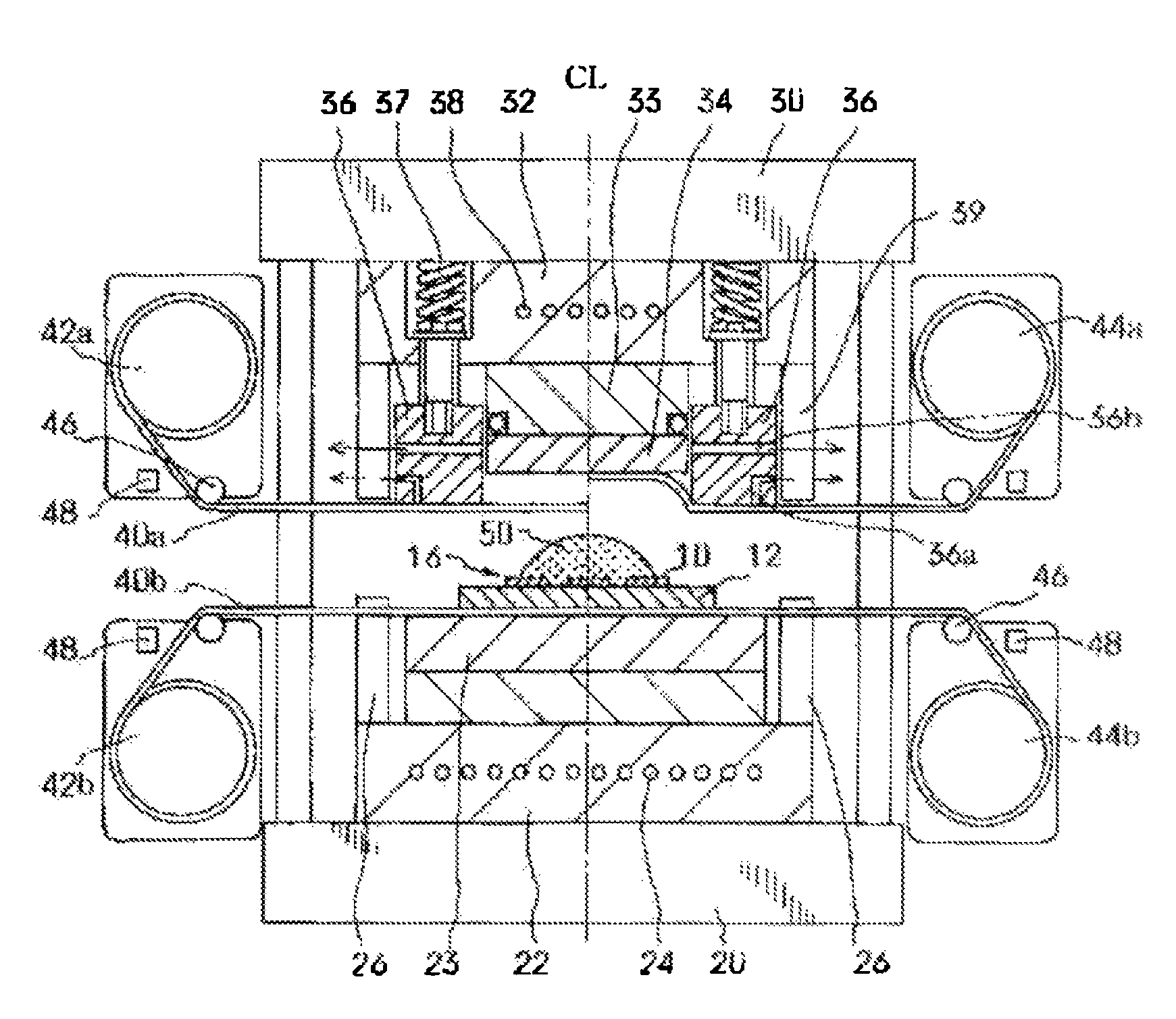
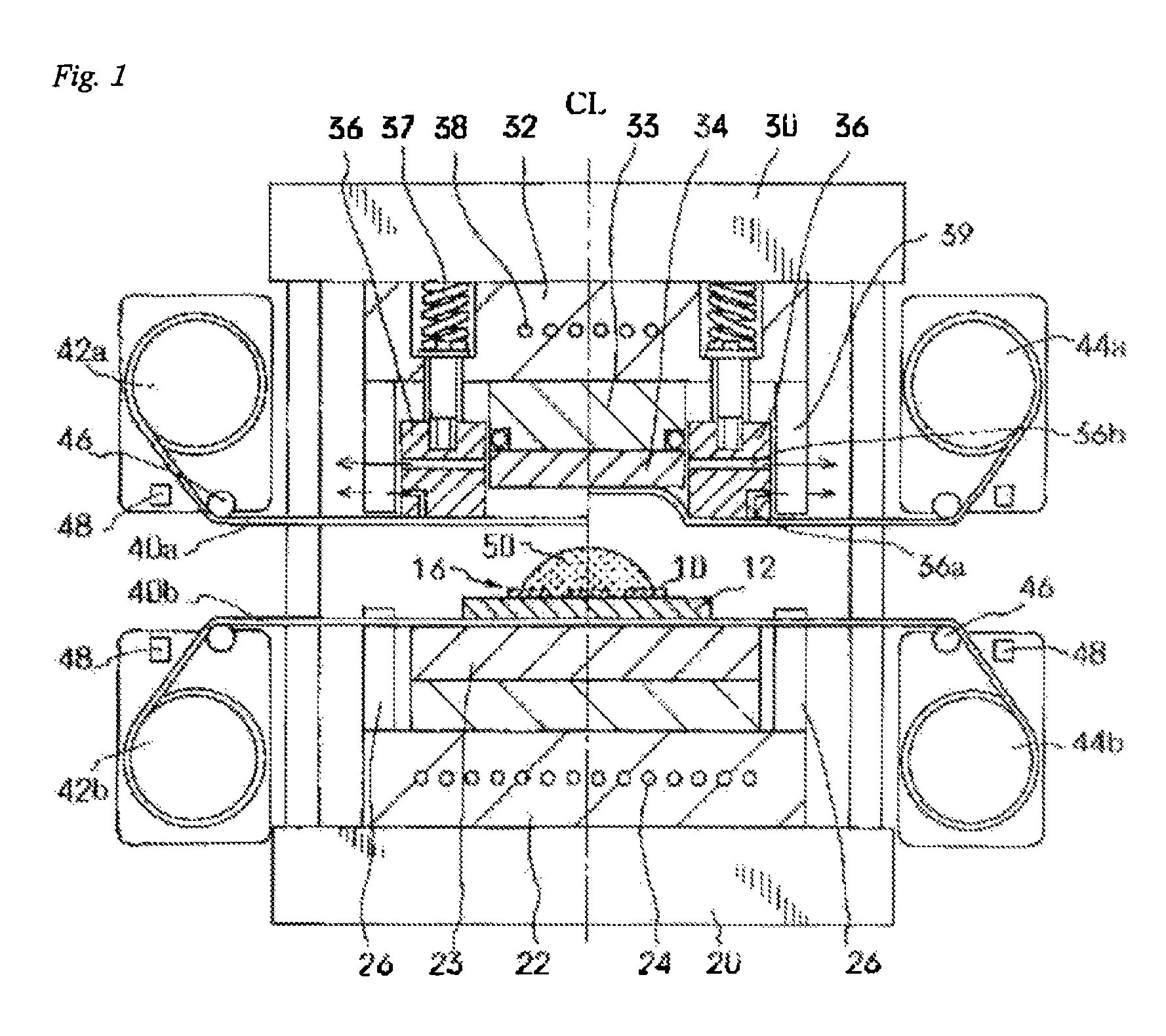
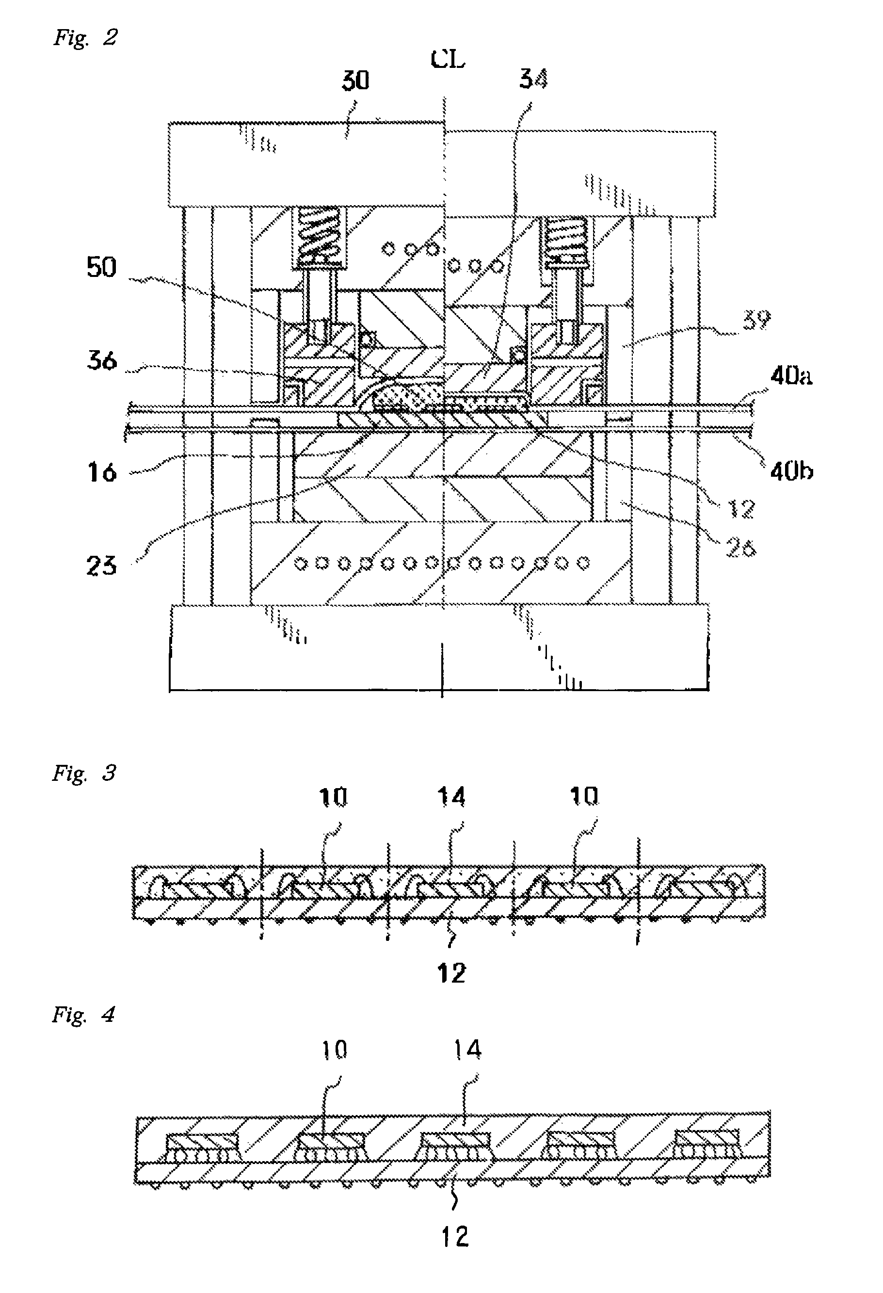
[0059]In the present practical example, a semiconductor device of the type shown in FIG. 3 was used. More specifically, (8 mm×14 mm) semiconductor chips 10 were fixed to a (70 mm×160 mm) printed circuit board made from a BT resin via a 35 μm-thick epoxy-resin die-bond agent layer. The printed circuit board was comprised of a laminated structure formed by applying an 18 μm-thick copper foil via an epoxy-resin adhesive layer having a 17 μm thickness onto one side of a 200 μm-thick BT resin film. Circuit patterns were then made from the aforementioned foil. Portions required for wire bonding of the circuit patterns were removed. The circuit patterns and bumps (not shown) of the semiconductor chips were electrically interconnected and wire bonded via 48 gold bonding wires. In total, 54 semiconductor chips divided into 3 blocks of 18 chips in each were secured to the printed circuit board and formed into respective wire patterns by wire bonding.

[0060]The hydrosilylatio...

example 2

Practical Example 2

[0061]A semiconductor device was prepared in the same manner as in Practical Example 1 with the exception that a hydrosilylation-curable liquid silicone rubber composition (B) was used instead of the hydrosilylation-curable liquid silicone rubber composition (A). Characteristics of the obtained semiconductor devices are shown in Table 2.


PUM

PropertyMeasurementUnit
torqueaaaaaaaaaa
torqueaaaaaaaaaa
viscosityaaaaaaaaaa

Abstract

A method of manufacturing a semiconductor device sealed in a cured silicone body by placing an unsealed semiconductor device into a mold and subjecting a curable liquid silicone composition that fills the spaces between the mold and the unsealed semiconductor device to compression molding under a predetermined molding temperature, wherein said curable liquid silicone composition has viscosity of 90 Pa·s or less at room temperature, a time interval from the moment directly after measurement of a torque with a curometer at the molding temperature to the moment when the torque reached 1 kgf·cm is not less than 1 min., while the time interval during which the torque grows from 1 kgf·cm to 5 kgf·cm is not more than 1 min.

Description

RELATED APPLICATIONS[0001]This application claims priority to and all the advantages of International Patent Application No. PCT / JP2005 / 004410, filed on Mar. 8, 2005, which claims priority to Japanese Patent Application No. JP2004-079597, filed on Mar. 19, 2004.TECHNICAL FIELD[0002]This invention relates to a method of manufacturing a semiconductor device and to a semiconductor device produced by the method.BACKGROUND ART[0003]Sealing of semiconductor devices is carried out with the use of a transfer-molding with a metal mold, potting with a liquid sealing resin, or screen-printing with a liquid sealing resin. The recent trend towards miniaturization of semiconductor devices demands that electronic devices be smaller in size, thinner in thickness, and allow resin sealing of packages as thin as 500 μm or thinner.[0004]If a transfer-molding is employed in resin sealing of thin packages, the thickness of the sealing resin could be precisely controlled, whereas there are problems that v...

Claims


Application Information

Patent Timeline
Patent Type & Authority Patents(United States)
IPC IPC(8): H01L23/29H01L21/56H01L23/31
CPCH01L21/566H01L23/296H01L24/97H01L23/3121H01L2224/16225H01L2224/45144H01L2224/48091H01L2224/48227H01L2224/73204H01L2924/15311H01L2224/32225H01L2924/00014H01L2924/00H01L2924/12042H01L2924/181H01L21/56H01L23/29
Inventor MORITA, YOSHITSUGUNAKANISHI, JUNJIMINE, KATSUTOSHI
Owner DOW TORAY CO LTD
Why Eureka
Try Eureka