Hybrid orientation accumulation mode GAA CMOSFET
a technology of cmosfet and orientation accumulation mode, which is applied in the direction of basic electric elements, electrical apparatus, and semiconductor devices, can solve the problems of low carrier mobility, low leakage current, and low device performance, and achieve high carrier mobility, reduce low-frequency noise, and high integration
- Summary
- Abstract
- Description
- Claims
- Application Information
AI Technical Summary
Benefits of technology
Problems solved by technology
Method used
Image
Examples
first embodiment
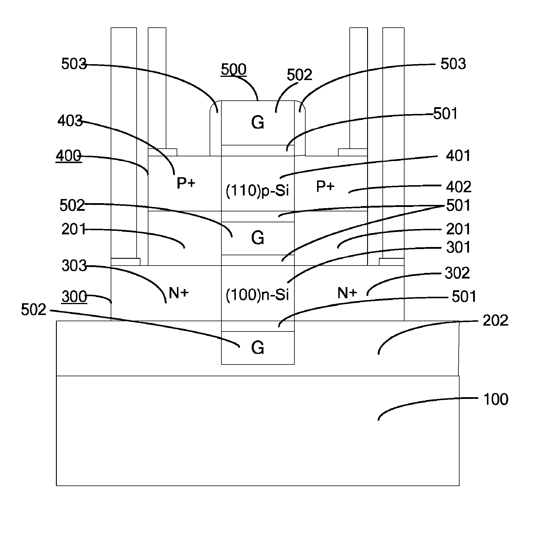
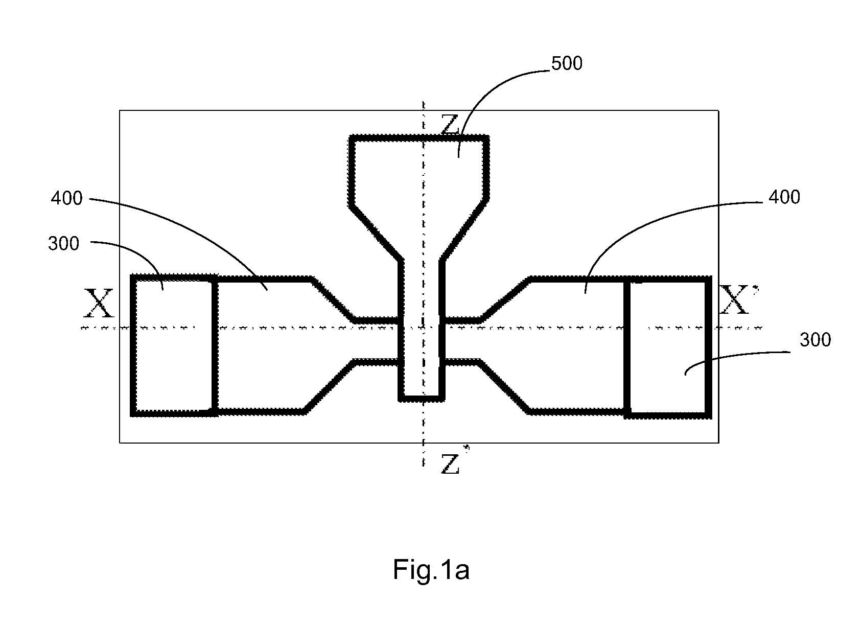
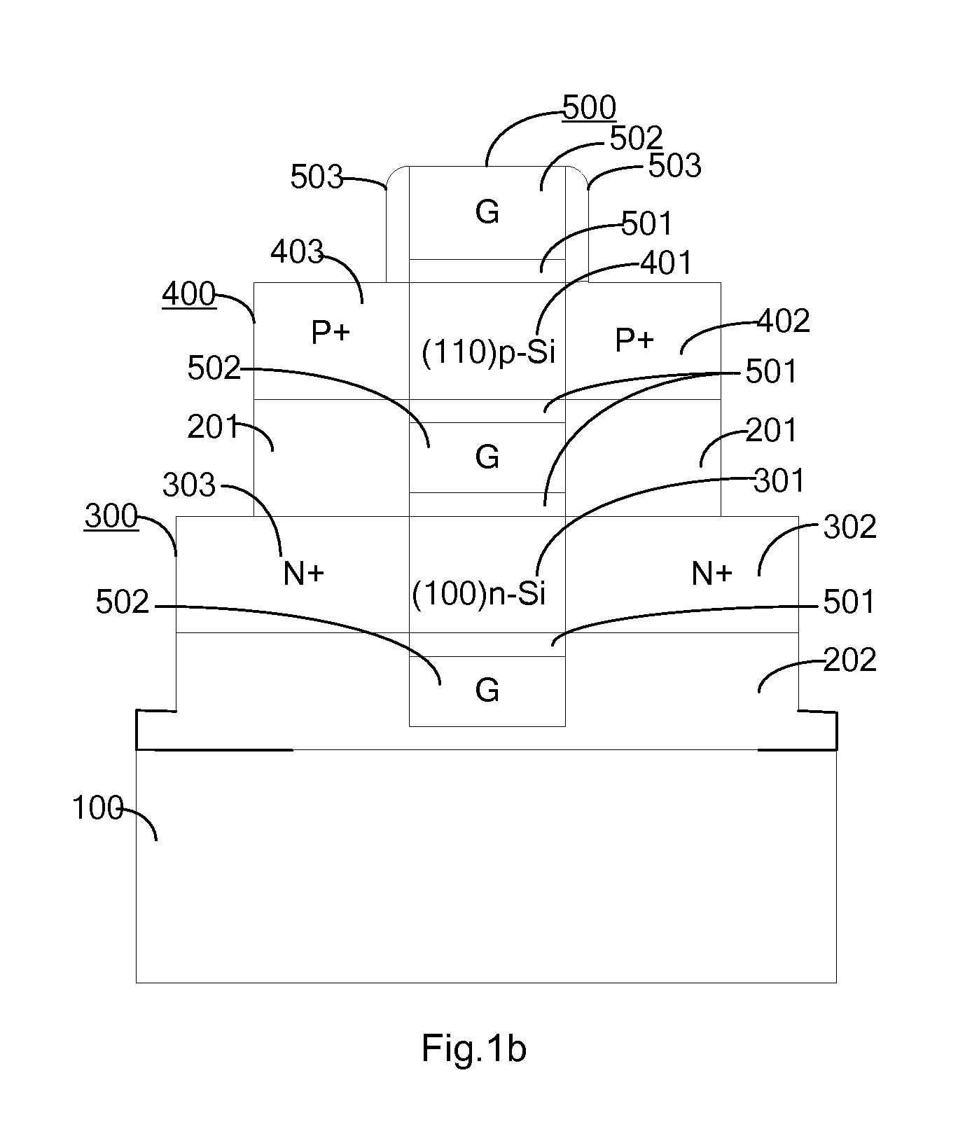
[0021]Referring to FIGS. 1a-1c, a hybrid orientation accumulation mode GAA CMOSFET of the first embodiment includes: a semiconductor substrate 100, a PMOS region 400 having a channel 401, an NMOS region 300 having a channel 301, and a gate region 500. Each of the channels 401, 301 has a racetrack-shaped cross section. The channel 401 is preferably formed of p-type Si(110) and the second channel 301 is preferably formed of n-type Si(100). The gate region 500 substantially surrounds the surfaces of the channels 401, 301. The racetrack-shaped cross section of the channels 401, 301 has a rectangular central portion and two substantially semicircular end portions contacting the opposite sides of the rectangular central portion. As shown in FIG. 3, the device is equivalent to a dual-gate channel structure and a GAAC structure, which are operated independently, wherein d is the diameter of the two semicircular end portions, w is the width of the rectangular central portion, the overall wid...
second embodiment
[0026]FIGS. 5a-5c shows another embodiment of the device. The hybrid orientation accumulation mode GAA CMOSFET includes: a semiconductor substrate100′, a PMOS region 400′ having a channel 401′, an NMOS region 300′ having a channel 301′, and a gate region 500′. The channel 401′ and the channel 301′ each has a racetrack-shaped cross section having a rectangular central portion and two semicircular end portions contacting the opposite ends of the rectangular central portion, and the channel 401′ is made of a semiconductor material different from the channel 301′. In the present embodiment, the channel 401′ is preferably formed of p-type Si(110) and the channel 301′ is preferably formed of n-type Si(100). The gate region 500′ surrounds the surfaces of the channels 401′, 301′. A first buried oxide (BOX) layer 201′ is disposed between the PMOS region 400′ and the NMOS region 300′, other than the gate region 500′, to avoid inter-region interference. A second buried oxide (BOX) layer 202′ i...
PUM
 Abstract
Description
Claims
Application Information


