Optical device with wavelength selective reflector

a wavelength selective reflector and optical device technology, applied in the field of lighting techniques, can solve the problems of achieving high intensity, reducing efficiency, and reducing efficiency, so as to achieve the effect of improving efficiency and being easy to implemen

Active Publication Date: 2012-09-18
KORRUS INC
View PDF30 Cites 44 Cited by
  • Summary
  • Abstract
  • Description
  • Claims
  • Application Information

AI Technical Summary

Benefits of technology

[0008]The present invention relates generally to lighting techniques and more particularly to techniques for transmitting electromagnetic radiation from LED devices, such as ultra-violet, violet, blue, blue and yellow, or blue and green, fabricated on bulk semipolar or nonpolar materials with use of entities such as phosphors, which emit light in a reflection mode. In other embodiments, the starting materials can include polar gallium nitride containing materials, and others. Merely by way of example, the invention can be applied to applications such as white lighting, multi-colored lighting, general illumination, decorative lighting, automotive and aircraft lamps, street lights, lighting for plant growth, indicator lights, lighting for flat panel displays, other optoelectronic devices, and the like.
[0009]According to an embodiment, the present invention provides an optical device. The device includes a substrate member having a surface region. The device also includes at least one LED configured overlying one or more portions of the surface region. The device further includes a spacer member having two or more sidewalls, the sidewall being characterized by an angle. The device additionally includes a wavelength conversion material disposed overlying the one or more sidewalls. The device also includes an optical member having a wavelength selective surface configured to block substantially direct emission of the at least one LED and configured to transmit at least one selected wavelength of reflected emission caused by an interaction with the wavelength conversion material.
[0010]According to another embodiment, the present invention provides an optical device. The device includes a substrate member having a surface region. The device also includes at least one LED configured overlying one or more portions of the surface region. The device further includes a wavelength conversion material disposed over the surface region. Additionally, the device includes an optical member having a wavelength selective surface configured to block substantially direct emission of the at least one LED and configured to transmit at least one selected wavelength of reflected emission caused by an interaction with the wavelength conversion material.
[0011]One or more benefits may be achieved using one or more of the specific embodiments. As an example, the present device and method provides for an improved lighting technique with improved efficiencies. In other embodiments, the present method and resulting structure are easier to implement using conventional technologies. In a specific embodiment, a blue LED device is capable of emitting electromagnetic radiation at a wavelength range from about 450 nanometers to about 495 nanometers and the yellow-green LED device is capable of emitting electromagnetic radiation at a wavelength range from about 495 nanometers to about 590 nanometers, although there can also be some variations.

Problems solved by technology

Unfortunately, the conventional light bulb dissipates more than 90% of the energy used as thermal energy.
Additionally, the conventional light bulb routinely fails often due to thermal expansion and contraction of the filament element.
Unfortunately, achieving high intensity, high-efficiency GaN-based green LEDs has been particularly problematic.
The performance of optoelectronic devices fabricated on conventional c-plane GaN suffer from strong internal polarization fields, which spatially separate the electron and hole wave functions and lead to poor radiative recombination efficiency.
Since this phenomenon becomes more pronounced in InGaN layers with increased indium content for increased wavelength emission, extending the performance of UV or blue GaN-based LEDs to the blue-green or green regime has been difficult.
Furthermore, since increased indium content films often require reduced growth temperature, the crystal quality of the InGaN films is degraded.
The difficulty of achieving a high intensity green LED has lead scientists and engineers to the term “green gap” to describe the unavailability of such green LED.
In addition, the light emission efficiency of typical GaN-based LEDs drops off significantly at higher current densities, as are required for general illumination applications, a phenomenon known as “roll-over.” Other limitations with blue LEDs using c-plane GaN exist.
These limitations include poor yields, low efficiencies, and reliability issues.

Method used


Image

  • Optical device with wavelength selective reflector
  • Optical device with wavelength selective reflector
  • Optical device with wavelength selective reflector

Examples


Embodiment Construction

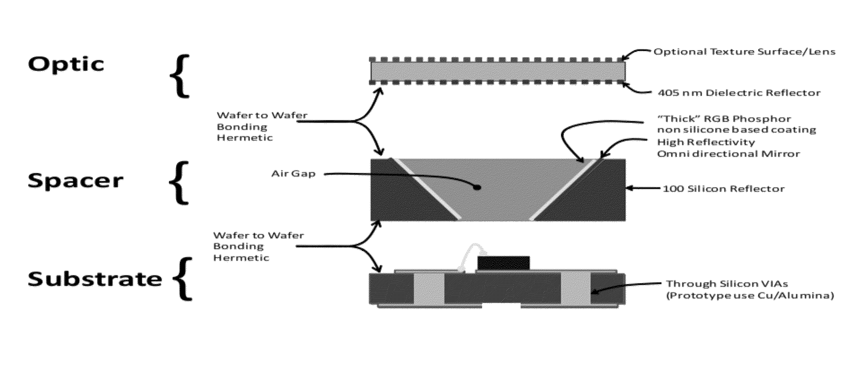
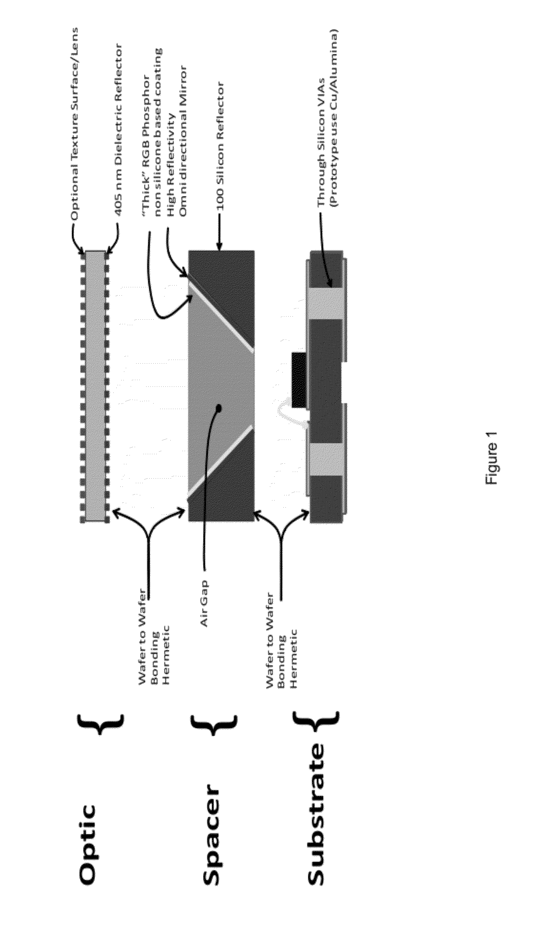
[0024]As explained above, conventional LED based optical devices are often inadequate. One of the challenges has been that light emitted by LED devices not being efficiently emitted. More specifically, an LED device is positioned on a substrate and covered by an optic. FIG. 1 is a simplified diagram illustrating an LED package according to an embodiment of the present invention. As shown in FIG. 1, the LED package comprises an optic, a spacer, and a substrate. An LED device is positioned on the substrate. Among other things, the LED package is configured to achieve a high efficiency where the phosphor operates in reflection. In one embodiment, these components are fabricated at the wafer level and assembled before division into individual parts.

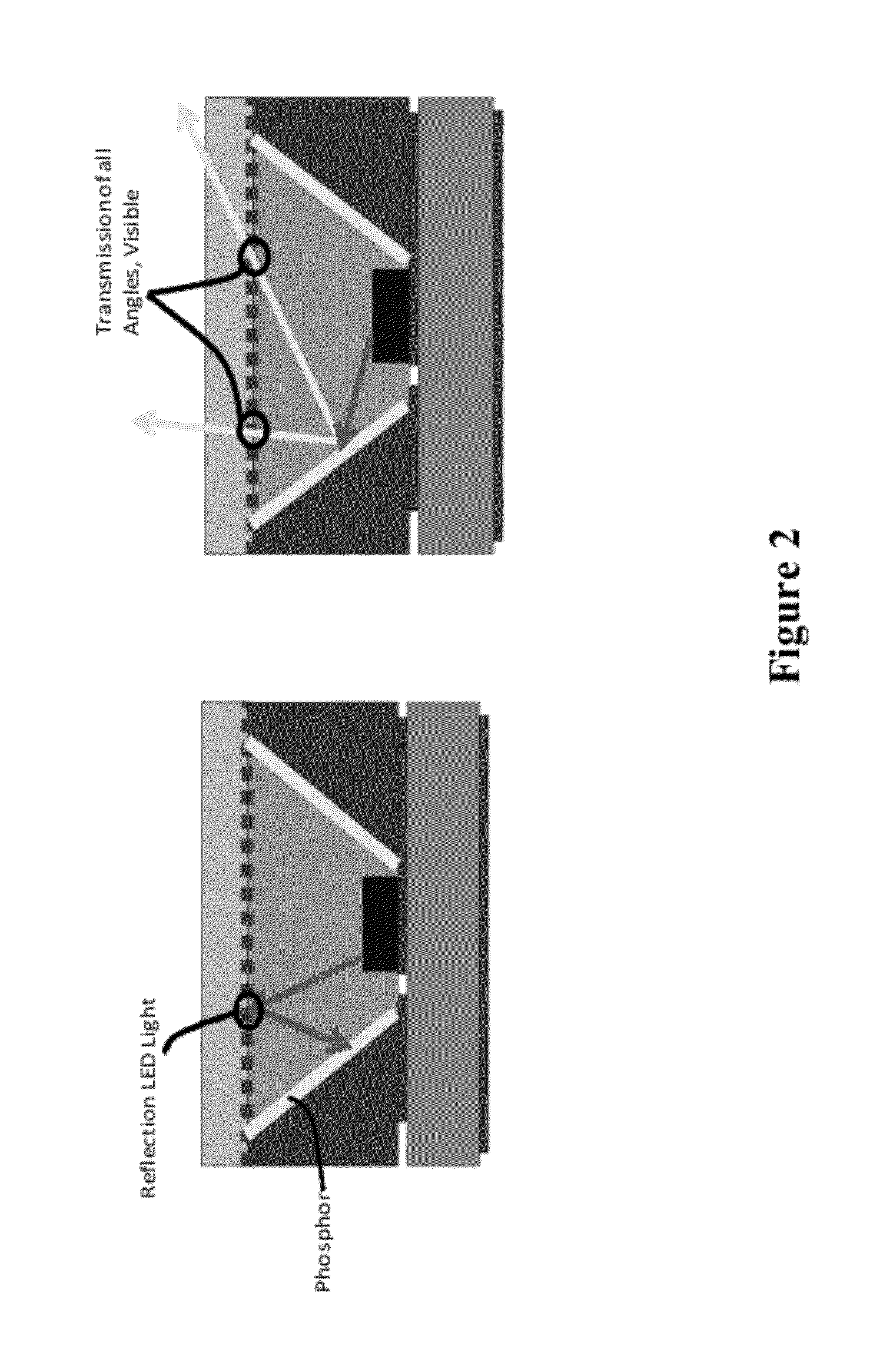
[0025]FIG. 2 is a simplified diagram illustrating light path in an LED package. As shown in FIG. 2, the bottom layer of the optic is coated with a dielectric filter. The dielectric is a long pass filter where it reflects the majority of LED l...


PUM


Abstract

Techniques are disclosed for transmitting electromagnetic radiation from LED devices, such as ultra-violet, violet, blue, blue and yellow, or blue and green, fabricated on bulk semipolar or nonpolar materials with phosphors. The starting material include polar gallium nitride.

Description

CROSS-REFERENCE TO RELATED APPLICATIONS[0001]This application claims priority to U.S. Provisional Patent Application No. 61 / 257,298, filed Nov. 2, 2009; U.S. Provisional Patent Application No. 61 / 257,303, filed Nov. 2, 2009; and U.S. Provisional Patent Application No. 61 / 256,934, filed Oct. 30, 2009, each of which is commonly owned, and hereby incorporated by reference for all purposes.BACKGROUND OF THE INVENTION[0002]This invention relates generally to lighting techniques, and more particularly to techniques for transmitting electromagnetic radiation from LED devices, such as ultra-violet, violet, blue, blue and yellow, or blue and green, fabricated on bulk semipolar or nonpolar materials with use of entities such as phosphors, which emit light in a reflection mode. In other embodiments, the starting materials can include polar gallium nitride containing materials, and others. Merely by way of example, the invention can be applied to applications such as white lighting, multi-color...

Claims


Application Information

Patent Timeline
Patent Type & Authority Patents(United States)
IPC IPC(8): H01L33/00
CPCH01L33/44H01L33/507H01L33/54
Inventor SHUM, FRANK TIN CHUNG
Owner KORRUS INC
Why Eureka
Try Eureka