Semiconductor chip, electrode structure therefor and method for forming same

a technology of semiconductor devices and electrodes, applied in the field of semiconductor devices, can solve problems such as and achieve the effect of preventing short circuit between bumps and preventing a phenomenon (migration)

Active Publication Date: 2012-09-18
TAIWAN SEMICON MFG CO LTD
View PDF23 Cites 1 Cited by
  • Summary
  • Abstract
  • Description
  • Claims
  • Application Information

AI Technical Summary

Benefits of technology

[0032]With this arrangement, electrical connection between the semiconductor chip and the solid device is properly established. Further, it is possible to prevent a phenomenon (migration) such that the metal atoms contained in the metal material of the bump migrate into the anisotropic conductive film as the resin layer. Therefore, the inter-bump short circuit is prevented which may otherwise occur due to that phenomenon.

Problems solved by technology

However, the metal as a material for the bumps (a metal constituent contained in the bumps) is liable to migrate, so that the reduction of the pitch of the bumps may lead to short circuit between the bumps due to the migration.

Method used


Image

  • Semiconductor chip, electrode structure therefor and method for forming same
  • Semiconductor chip, electrode structure therefor and method for forming same
  • Semiconductor chip, electrode structure therefor and method for forming same

Examples


Embodiment Construction

[0044]Embodiments of the present invention will hereinafter be described in detail with reference to the attached drawings.

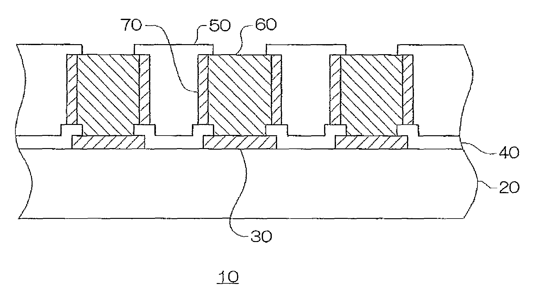
[0045]FIG. 1 is a schematic sectional view for explaining the construction of a semiconductor device according to one embodiment of the present invention. The semiconductor device has a so-called chip-on-chip structure, in which a secondary chip 2 is bonded onto a primary chip 1.

[0046]The primary chip 1 and the secondary chip 2 are each a semiconductor chip (e.g., a silicon chip). The primary chip 1 and the secondary chip 2 are bonded to each other in face-to-face relation with an active surface of the primary chip 1 (on the side of the surface of an active region formed with a device) being opposed to an active surface of the secondary chip 2. More specifically, the primary chip 1 is die-bonded to an island portion 4 of a lead frame 3 with its active surface facing up. The secondary chip 2 is bonded to the upper surface of the primary chip 1 with its face down....


PUM


Abstract

A semiconductor chip, an electrode structure and a method of manufacture, the chip including a semiconductor substrate having a multi-level interconnection and an electrode pad connected to the interconnection, a protective film on the substrate, an insulating film on the protective film, a bump of a metal on the electrode pad, and a barrier layer between the side of the bump and the insulation film.

Description

CROSS-REFERENCE TO RELATED APPLICATIONS[0001]This application is a division of application Ser. No. 11 / 794,243, filed on Jun. 27, 2007, now issued as U.S. Pat. No. 7,956,460. Furthermore, this application claims the benefit of priority of Japanese applications 2004-381363, filed Dec. 28, 2004 and 2005-129000, filed Apr. 27, 2005. The disclosure of Japanese application 2004-381363 is incorporated herein by reference.BACKGROUND OF THE INVENTION[0002]1. Field of the Invention[0003]The present invention relates to a semiconductor chip and a production method therefor, an electrode structure provided in the semiconductor chip and a formation method therefor, and a semiconductor device having a chip-on-chip structure or a flip chip bonding structure.[0004]2. Description of the Related Art[0005]A known method for connecting a semiconductor chip to a wiring board (mounting board) in a semiconductor device such as an IC or an LSI is to bond bumps provided on a surface of the semiconductor ch...

Claims


Application Information

Patent Timeline
Patent Type & Authority Patents(United States)
IPC IPC(8): H01L23/48H01L21/44
CPCH01L24/11H01L25/0657H01L24/13H01L23/49575H01L24/83H01L2224/114H01L2224/116H01L2224/13099H01L2224/13144H01L2224/13147H01L2224/16145H01L2224/48091H01L2224/48247H01L2224/83851H01L2225/0651H01L2225/06513H01L2225/06582H01L2924/01013H01L2924/01022H01L2924/01027H01L2924/01029H01L2924/01074H01L2924/01078H01L2924/01079H01L2924/01082H01L2924/14H01L2924/00014H01L2924/01005H01L2924/01006H01L2924/01033H01L2924/014H01L2924/3512H01L2924/00H01L2224/2929H01L2224/293H01L2924/10253H01L24/05H01L2224/05124H01L2224/05567H01L2224/05573H01L2224/05624H01L2224/05647H01L2924/01014
Inventor NAKATANI, GORO
Owner TAIWAN SEMICON MFG CO LTD
Why Eureka
Try Eureka