

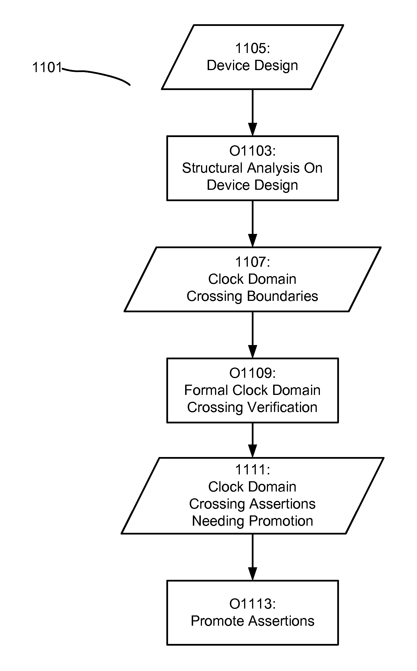
Formal verification of clock domain crossings
a clock domain and domain technology, applied in error detection/correction, program control, instruments, etc., can solve problems such as domain crossing, synchronizer scheme, and design where multiple clock domain crossings are difficult for designers to verify
- Summary
- Abstract
- Description
- Claims
- Application Information
AI Technical Summary
Benefits of technology
Problems solved by technology
Method used
Image

Examples
Embodiment Construction
[0033]The disclosed technology includes all novel and unobvious features, aspects, and embodiments of the systems and methods described herein, both alone and in various combinations and sub-combinations thereof. The disclosed features, aspects, and embodiments can be used alone or in various novel and unobvious combinations and sub-combinations with one another.
[0034]Although the operations of the disclosed methods are described in a particular sequential order for convenient presentation, it should be understood that this manner of description encompasses rearrangements, unless a particular ordering is required by specific language set forth below. For example, operations described sequentially may in some cases be rearranged or performed concurrently. Moreover, for the sake of simplicity, the disclosed flow charts and block diagrams typically do not show the various ways in which particular methods can be used in conjunction with other methods. Additionally, the detailed descript...
PUM
 Abstract
Description
Claims
Application Information