

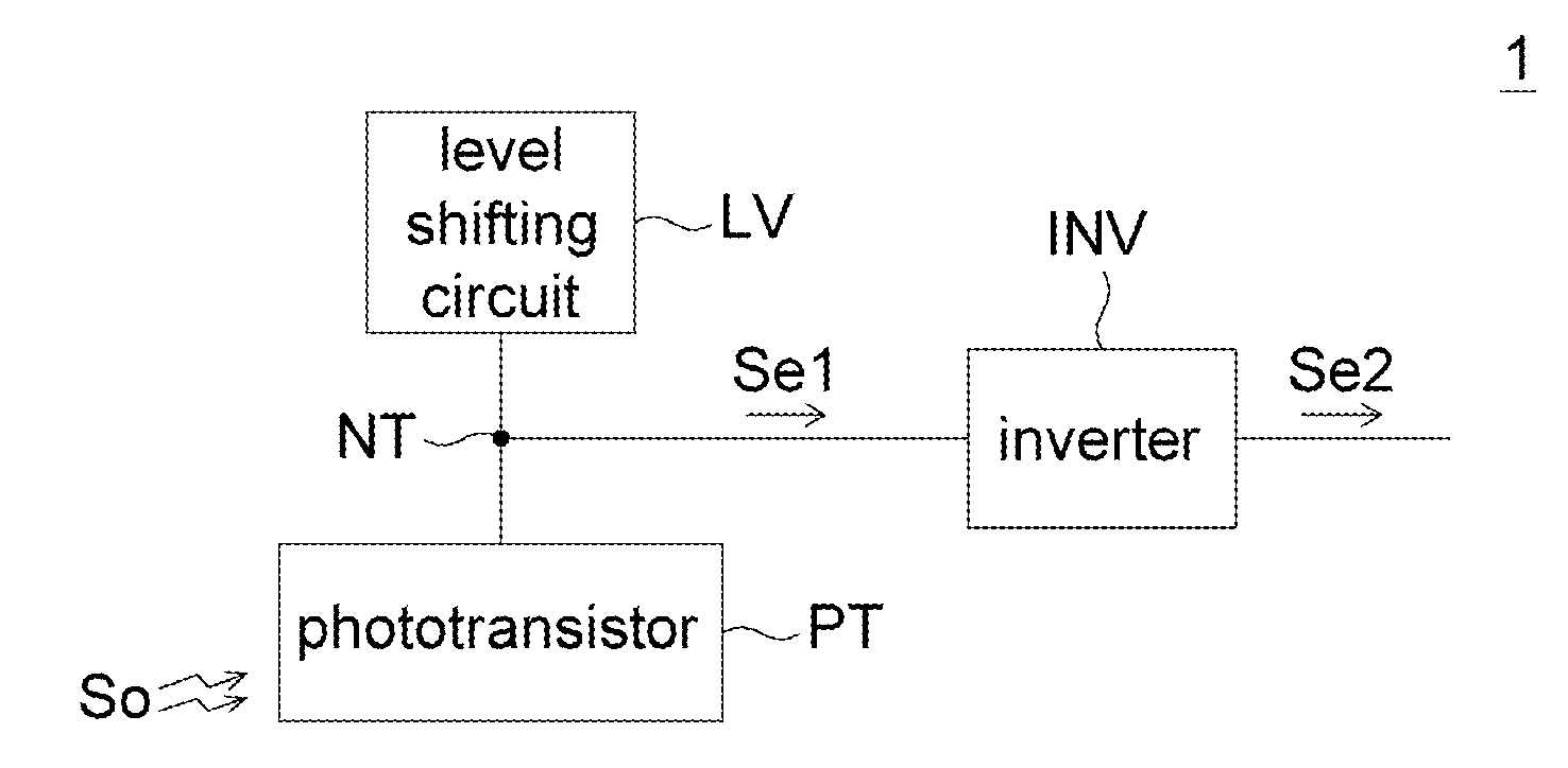
Photosensor circuit having a level shifting circuit for biasing a first node with an operation voltage signal and a phototransistor for modulating the level of the operation voltage signal
a photosensor and level shifting technology, applied in the field of photosensor circuits, can solve the problems of higher manufacturing cost and achieve the effect of lowering cost and lowering temperature process
- Summary
- Abstract
- Description
- Claims
- Application Information
AI Technical Summary
Benefits of technology
Problems solved by technology
Method used
Image

Examples
first embodiment
[0018
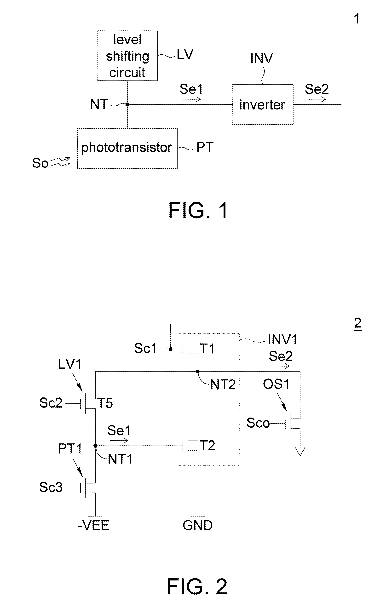
[0019]Referring to FIG. 2, a circuit diagram of a photosensor circuit according to a first embodiment of the invention is shown. The photosensor circuit 2 includes a node NT1, a level shifting circuit LV1, a phototransistor PT1 and an inverter INV1, wherein the node NT1 has an operation voltage signal.
[0020]For example, the active layer of the phototransistor PT1 is made with amorphous silicon or organic semiconductor, and the phototransistor can be implemented on a flexible plastic substrate. The level shifting circuit LV1 and the inverter INV1 are both implemented by transistors. For example, the transistors of the level shifting circuit LV1 and the inverter INV1 are implemented by metal-oxide thin film transistors.
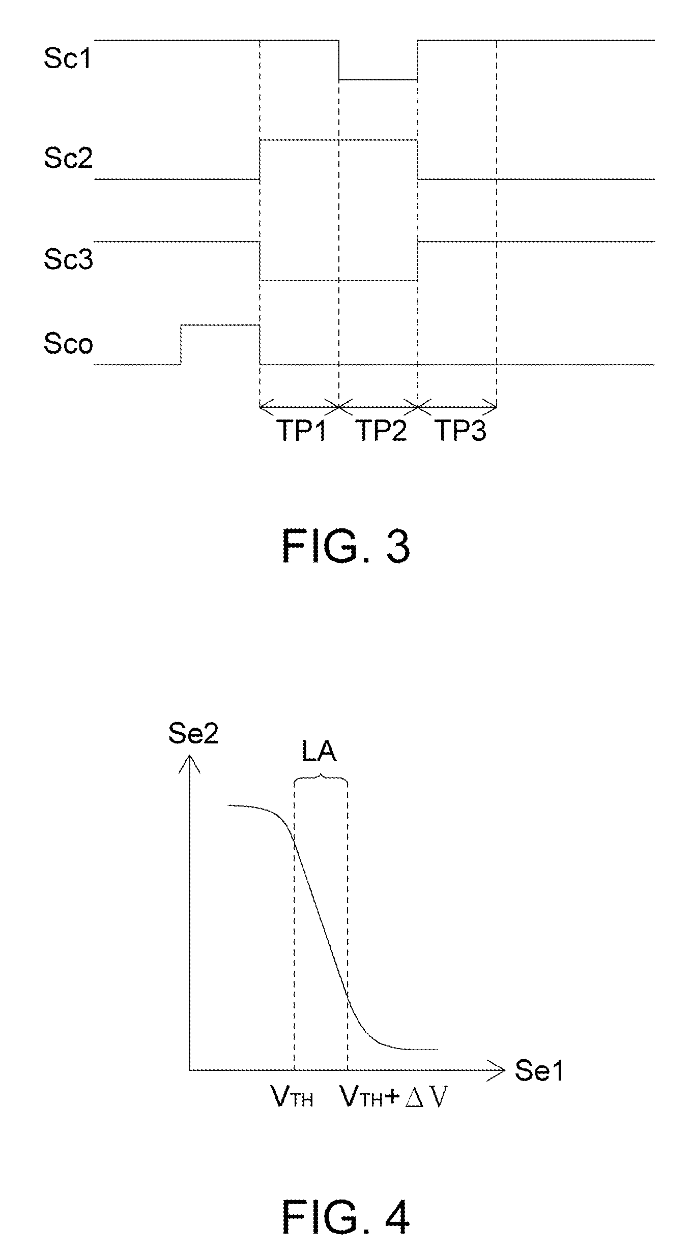
[0021]The inverter INV1 includes a node NT2, and transistors T1 and T2. The node NT2 has an electrical signal Se2. The drain and the gate of the transistor T1 receive a control signal Sc1, and the source of the transistor T1 is coupled to the node NT2. On the part ...
second embodiment
[0033
[0034]Referring to FIG. 6, a circuit diagram of a photosensor circuit according to a second embodiment of the invention is shown. The photosensor circuit 4 according to the present embodiment of the invention is different from the photosensor circuit of the first embodiment in that the drain of the level shifting circuit LV2 is not coupled to the node NT2″ but receives a bias signal Vrf instead. Thus, the level shifting circuit LV2 directly receives the reset voltage signal Sr via the gate and is accordingly turned on to bias the operation voltage signal on the node NT1′ to the level of the input signal bias signal Vrf without using the timing control of the control signals Sc1-Sc3.
[0035]The photosensor circuits according to the above embodiments of the invention employ phototransistors as photosensing elements, and employ amplifiers implemented with inverters for amplifying electrical signals generated by the phototransistors in response to the sensed optical signals. Thus, in...
PUM
 Abstract
Description
Claims
Application Information