

Semiconductor device manufacturing method
a manufacturing method and semiconductor technology, applied in the manufacture of microstructural devices, microstructured devices, electric devices, etc., can solve the problems of low volatility of iii-v group materials, low volatility of compound semiconductors, and difficult anisotropic processing
- Summary
- Abstract
- Description
- Claims
- Application Information
AI Technical Summary
Benefits of technology
Problems solved by technology
Method used
Image

Examples
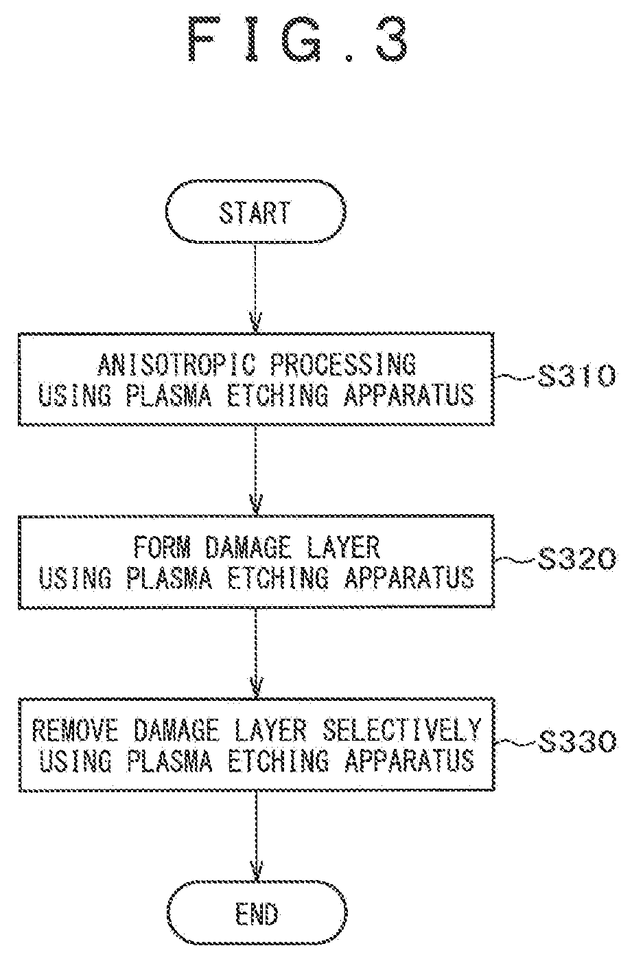
first embodiment
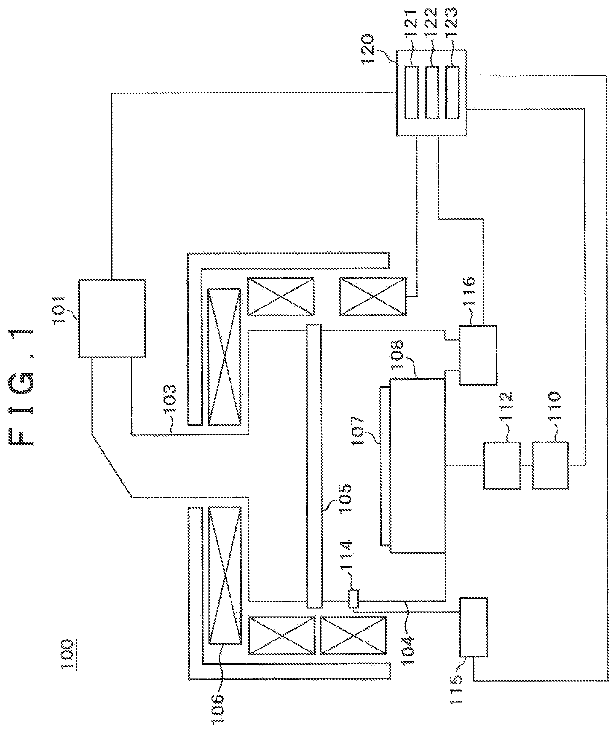
[0030]FIG. 1 is a block diagram which shows the structure of the plasma etching apparatus 100 used for the plasma etching process and the damage layer forming process in this embodiment.
[0031]The plasma etching apparatus 100 shown in FIG. 1 according to this embodiment includes: an etching chamber 104; a microwave power source 101; a waveguide 103 connecting the microwave power source 101 with the etching chamber 104; a dielectric window 105 for supplying the etching gas introduced into the etching chamber 104 in the upper part of the etching chamber 104 to the etching chamber 104 and introducing the microwave power, for example, with a frequency of 2.45 GHz, propagated from the waveguide 103 into the etching chamber 104; and electromagnetic coils 106 arranged around the etching chamber 104 to generate a magnetic field in the etching chamber 104, so that a microwave ECR plasma is generated in the etching chamber 104.
[0032]A sample holder 108 on which a sample 107 is placed is provid...
second embodiment
[0111]Whereas the first embodiment concerns a method in which anisotropic processing and damage layer formation are performed using the plasma etching apparatus 100 and the damage layer is selectively removed by the wet etching process using the wet etching apparatus 200, the second embodiment concerns a method in which the damage layer is removed by reaction with radicals.
[0112]In the second embodiment, the anisotropic processing and damage layer formation process which are performed using the plasma etching apparatus 100 are the same as in the first embodiment and description thereof is omitted.
[0113]FIG. 10 shows the structure of a plasma processing apparatus 1000 for removing the damage layer by reaction with radicals which is used in this embodiment.
[0114]The plasma processing apparatus 1000 according to this embodiment includes a plasma processing chamber 1100 comprised of a plasma generating chamber 1110 and a radical radiation chamber 1120 and in the radical radiation chambe...
PUM
| Property | Measurement | Unit |
|---|---|---|
| frequency | aaaaa | aaaaa |
| aspect ratio | aaaaa | aaaaa |
| aspect ratio | aaaaa | aaaaa |
Abstract
Description
Claims
Application Information