Process of packaging organic electroluminescent panel

a technology of electroluminescent panels and organic electroluminescent layers, which is applied in the direction of printed circuit manufacturing, solid-state devices, printed circuit assembling, etc., can solve the problems of warpage of assembly substrates, adversely affecting the organic electroluminescent layer of organic electroluminescent panels, and the limitation of size, so as to reduce the stress of protective layers and improve thermal dissipation characteristics

Inactive Publication Date: 2005-01-25
III HLDG 1
View PDF9 Cites 0 Cited by
  • Summary
  • Abstract
  • Description
  • Claims
  • Application Information

AI Technical Summary

Benefits of technology

Therefore, the object of the present invention is to provide a process of packaging an organic electroluminescent panel, which can reduce the stress of the protective layer and improve the thermal dissipation characteristics.
Another object of the present invention is to provide a process of packaging an organic electroluminescent panel, which is a low-temperature and low-stress package process suitable for the low temperature process of organic electroluminescent panels.

Problems solved by technology

The prior art package structure of the organic electroluminescent panel can integrate the driving IC therewith; however, it will be confronted with the limitation of size.
The prior art package structure of the organic electroluminescent panel can integrate a plurality of panels and has a large size; however, the high-temperature reflow process for connecting the pads and bumps will result in warpage of the assembly substrate.
Moreover, the high-temperature reflow process adversely affects the organic electroluminescent layer of the organic electroluminescent panel.

Method used


Image

  • Process of packaging organic electroluminescent panel
  • Process of packaging organic electroluminescent panel
  • Process of packaging organic electroluminescent panel

Examples


first embodiment

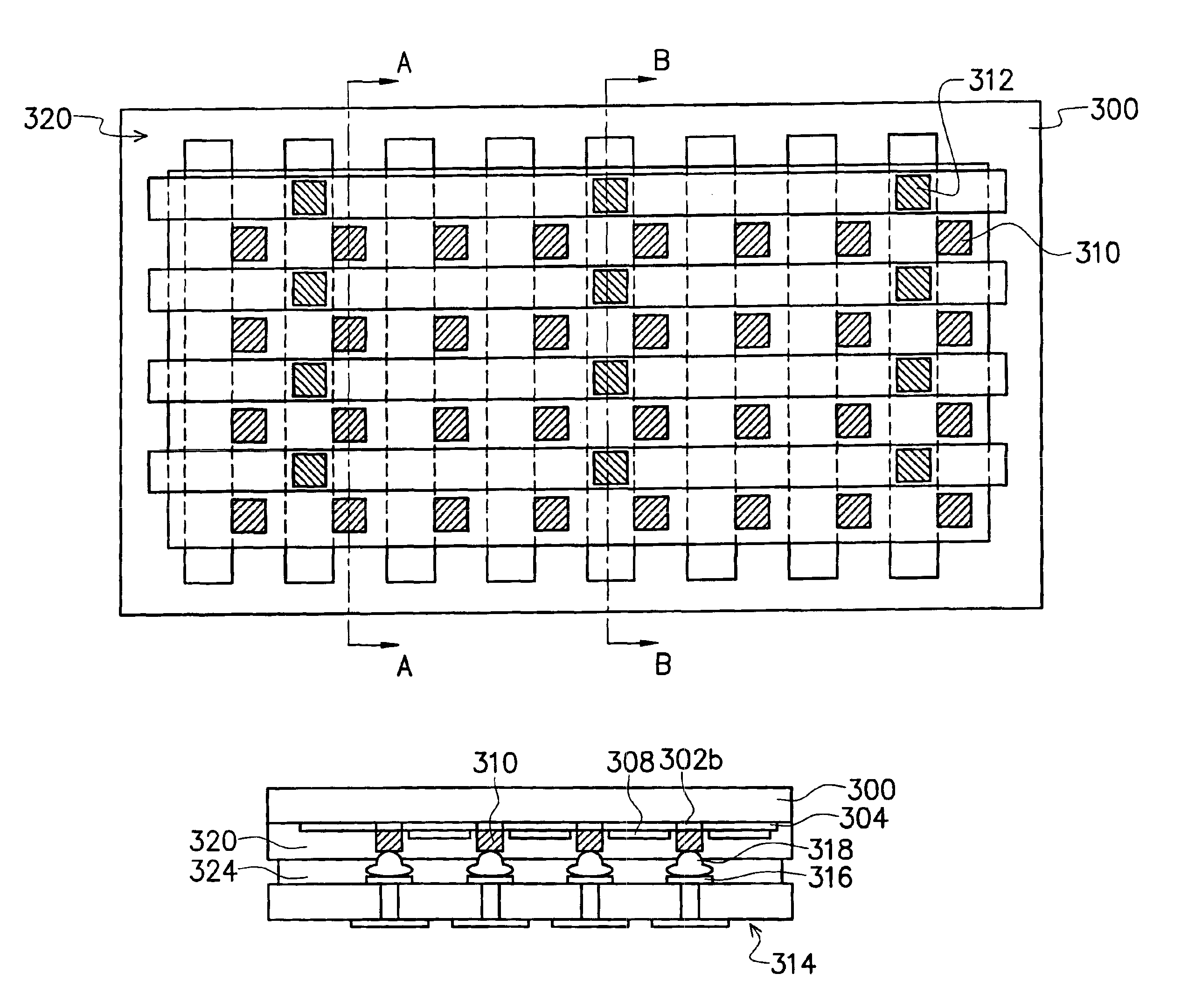
Referring to FIGS. 3-6, schematic views showing progression of steps of a process of forming an organic electroluminescent panel according to the present invention is shown. Referring to FIG. 3, a transparent substrate 300 is provided, which is comprised of, for example, glass, acrylic or the other transparent material. A plurality of anodes 302 are formed on the transparent substrate 300, wherein each of the anodes has a driving area 302a and at least one connecting areas 302b. The anodes 302 are comprised of, for example, indium tin oxide (ITO) or the other transparent material. The driving area 302a is comprised of, for example, stripes and parallel to each other. The connecting area 302b are connected to the driving area 302a.

Please referring to FIG. 4, after the anodes 302 are formed over the transparent substrate 300, a patterned organic electroluminescent layer 304 is formed over the transparent substrate 300 or on the anodes 302. The patterned organic electroluminescent lay...

second embodiment

Referring to FIGS. 9-12, schematic views showing the progression of steps of a process of forming an organic electroluminescent panel according to the present invention is shown. Referring to FIG. 9, a transparent substrate 300 is provided, which is comprised of, for example, glass, acrylic or the other transparent material. A plurality of anodes 302 are formed on the transparent substrate 300, each of the anodes 302 comprises a driving area 302a and at least one connecting areas 302b. The anodes 302 are comprised of, for example, indium tin oxide (ITO) or the other transparent material. The driving areas 302a are, for example, stripes and are arranged parallel to each other. The connecting areas 302b are connected to the driving areas 302a, serving for connection to external circuits.

Referring to FIG. 10, after the anodes 302 are formed over the transparent substrate 300, a patterned organic electroluminescent layer 304 is formed over the transparent substrate 300. The patterned or...


PUM

PropertyMeasurementUnit
thicknessaaaaaaaaaa
thicknessaaaaaaaaaa
temperatureaaaaaaaaaa

Abstract

A process of packaging an OEL panel is disclosed. A printed circuit board is provided, wherein the printed circuit board comprises a plurality of bonding pads and a plurality of bumps on the bonding pads. Next, at least one OEL panel having a plurality of polysolder interconnections is provided. Next, the OEL panel disposed on the printed circuit board. A reflow process is performed so that the OEL panel can electrically connect with the PCB by the polysolder interconnections. Because of the low-temperature reflow process, the process of packaging an OEL panel can be accomplished by a low temperature process.

Description

CROSS-REFERENCE TO RELATED APPLICATIONThis application claims the priority benefit of Taiwan application serial no. 91124307, filed on Oct. 22, 2002.BACKGROUND OF THE INVENTION1. Field of the InventionThe present invention relates to a process of packaging an organic electroluminescent panel, and more particularly to a process of packaging an organic electroluminescent panel having a polysolder interconnection array.2. Description of the Related ArtAn organic electroluminescent (OEL) device includes two electrodes and an electroluminescent layer between the electrodes. When a current or voltage is applied to the device, holes from the anode will recombine with electrons from the cathode within the emitting layer and excite the molecules therein to the excited state. When the excited molecules release energy and return back to the ground state, a portion of energy generated therefrom will be released in the form of light. Because of its self-luminescence, wide viewing angle, fast res...

Claims


Application Information

Patent Timeline
Patent Type & Authority Patents(United States)
IPC IPC(8): H05K3/34
CPCH01L27/3288H01L27/3293H01L51/5237Y10T29/49169H01L2224/16225Y10T29/49144Y10T29/49149H05K3/3436H01L2924/12044H10K59/179H10K59/18H10K50/841H10K50/844H01L2924/00
Inventor WU, CHIN-LONGTANG, TUNG-YANGHSU, SHIH-MINGCHEN, SHANG-WEI
Owner III HLDG 1
Why Eureka
Try Eureka