Resistive memory device and method of fabricating the same

a memory device and resistive technology, applied in the field of resistive memory devices, can solve the problems of loss of stored data of memory devices and difficulty in achieving high integration

Active Publication Date: 2012-10-02
ELECTRONICS & TELECOMM RES INST
View PDF11 Cites 6 Cited by
  • Summary
  • Abstract
  • Description
  • Claims
  • Application Information

AI Technical Summary

Problems solved by technology

Volatile memory devices lose their stored data when their power supplies are interrupted, while nonvolatile memory devices retain their stored data even when their power supplies are interrupted.
However, because the flash memory is configured to accumulate electric charges on a floating gate at a high electric field, a cell structure becomes complex to cause difficulty in achieving high integration.

Method used


Image

  • Resistive memory device and method of fabricating the same
  • Resistive memory device and method of fabricating the same
  • Resistive memory device and method of fabricating the same

Examples


Embodiment Construction

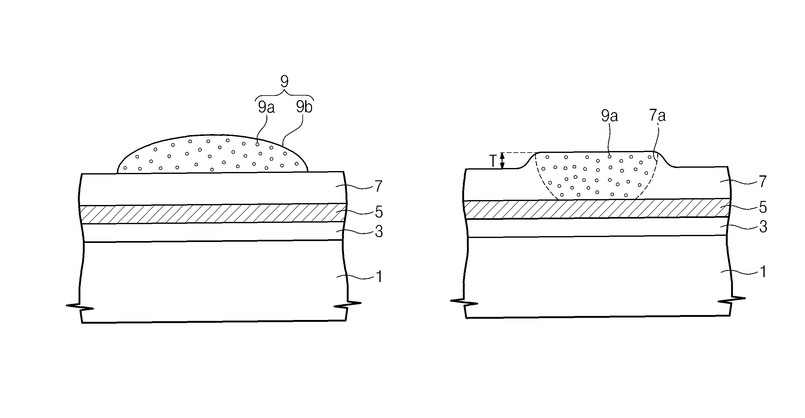
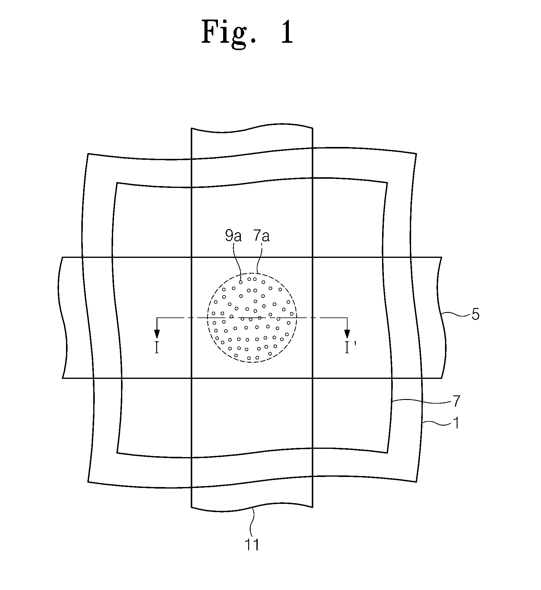
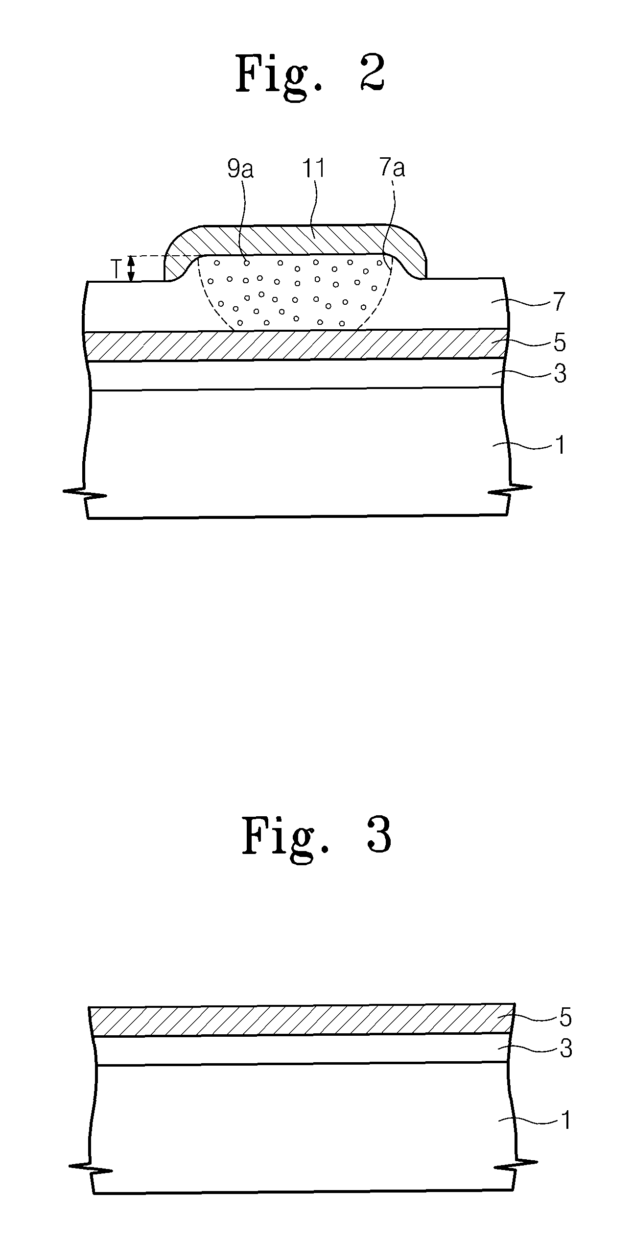
[0027]The inventive concept will now be described more fully hereinafter with reference to the accompanying drawings, in which preferred embodiments of the inventive concept are shown. However, the inventive concept may be embodied in many different forms and should not be construed as limited to the embodiments set forth herein. Rather, these embodiments are provided so that this disclosure will be thorough and complete, and will fully convey the scope of the inventive concept to those skilled in the art. Like numbers refer to like elements throughout.

[0028]In the specification, the dimensions of layers and regions are exaggerated for clarity of illustration. It will also be understood that when a layer (or film) is referred to as being “on” another layer or substrate, it can be directly on the other layer or substrate, or intervening layers may also be present. Also, though terms like a first, a second, and a third are used to describe various regions and layers in various embodim...


PUM

PropertyMeasurementUnit
viscosityaaaaaaaaaa
work functionaaaaaaaaaa
temperatureaaaaaaaaaa

Abstract

Provided are a resistive memory device and a method of fabricating the same. The resistive memory device comprises an electron channel layer formed by means of a swelling process and an annealing process. Thus, conductive nanoparticles are uniformly dispersed in the electron channel layer to improve reliability of the resistive memory device. According to the method, an electron channel layer is formed by means of a printing process, a swelling process, and an annealing process. Thus, fabrication time is reduced.

Description

CROSS-REFERENCE TO RELATED APPLICATIONS[0001]This U.S. non-provisional patent application claims priority under 35 U.S.C. §119 to Korean Patent Application No. 10-2010-0043570, filed on May 10, 2010, the entirety of which is hereby incorporated by reference.BACKGROUND[0002]1. Technical Field[0003]The present disclosure herein relates to nonvolatile memory devices and methods for fabricating the same and, more particularly, to a resistive memory device and a method for fabricating the same.[0004]2. Description of Related Art[0005]In recent years, dynamic random access memory (DRAM) devices, static random access memory (SRAM) devices, and flash memory devices have been widely used as semiconductor memory devices. These semiconductor memory devices may be classified into volatile memory devices and nonvolatile memory devices. Volatile memory devices lose their stored data when their power supplies are interrupted, while nonvolatile memory devices retain their stored data even when thei...

Claims


Application Information

Patent Timeline
Patent Type & Authority Patents(United States)
IPC IPC(8): H01L51/40
CPCG11C13/0007G11C13/0009G11C13/0011G11C13/0014H01L45/1233H01L45/14H01L45/1608H01L45/04G11C13/0016H10N70/20H10N70/881H10N70/021H10N70/826B82Y10/00
Inventor YANG, YONG SUKYOU, IN-KYUKOO, JAE BONJUNG, SOON WONKIM, KANG DAENOH, YONG-YOUNG
Owner ELECTRONICS & TELECOMM RES INST
Why Eureka
Try Eureka