Coated nanoparticles and quantum dots for solution-based fabrication of photovoltaic cells

a photovoltaic cell and nanoparticle technology, applied in the field of photovoltaic cells, can solve the problems of gallium oxide, potential explosive step, and use of metal oxides as precursor materials for cigs

Inactive Publication Date: 2007-12-11
AERIS CAPITAL SUSTAINABLE IP
View PDF93 Cites 237 Cited by
  • Summary
  • Abstract
  • Description
  • Claims
  • Application Information

AI Technical Summary

Problems solved by technology

However, there are several drawbacks to the use of metal oxides as precursor materials for CIGS solar cells.
First, the use of oxide-based particles in CIGS absorber layer construction requires a high-temperature hydrogen reduction step to reduce the oxides.
In addition to requiring substantial time and energy, this step is potentially explosive.
Further, although it is highly desirable to incorporate gallium in the active layer of the solar cells, the presence of gallium results in the formation of gallium oxide upon annealing, a highly stable material which is very difficult to reduce even under the most extreme conditions.
As a result, it is very difficult to effectively incorporate gallium into a nascent copper indium precursor film using a metal oxide synthesis approach.
In addition, the methods of particle formation and deposition taught in the prior art carry significant challenges.
For example, mechanical milling is a lengthy process that can requires substantial energy and take several tens of hours to achieve sub-micron sized particles.
Further, even after milling, particles are rarely uniform, resulting in a substantial size distribution, which can result in poorly packed precursor films, leading to low-density absorber layers with poor optoelectronic and electronic properties.
First, the ultrasonic spraying of thin layers of sub-micron sized particles onto a substrate is an inherently non-uniform process, resulting in differential drying rates as particles are spray deposited.
Non-uniform drying can result from any of several factors including but not limited to differential drying on the substrate, mid-stream drying (e.g. drying of droplets prior to reaching a substrate), and pooling of particles and droplets into non-contiguous aggregates that leave space between the aggregation loci.
Further, it is especially challenging to achieve any scaling for this technique since it is inherently difficult to carry out a uniform wet deposition of many small particle-containing droplets over a large area without any premature drying prior to completion of the deposition process.
Films are often uneven and have substantial spatial non-uniformities across their surface.
These and related forms of non-uniform drying lead to the formation of pockets and voids within the deposited film, creating a porous material which leads to a solar cell with poor and unstable optoelectronic and electronic properties.
Some of these defects can be overcome when much thicker films are deposited, e.g. in the 20 to 100 micron thick range, but such films are not useful for solar cell devices, which typically require the absorber layer to have a thickness between about one and two microns.
Rapid drying of thin films also limits the potential scaleability of spray deposition techniques.
This uneven drying results in additional spatial non-uniformities, pockets, and voids.
While the use of multiple spray heads concurrently moving across a substrate surface decreases the time required for deposition across the total surface area, local non-uniformities can arise from regions near each of the nozzles as well as in overlapping regions.
For sub-micron precursor particles formed by either mechanical milling or spray pyrolysis, it is difficult to make precisely-shaped and sized nanoparticles of indium and gallium since indium is so soft and gallium is molten at room temperature.
It is difficult to precisely tune the stoichiometry and / or phase of the nanoparticles on a nanometer scale with current techniques.

Method used


Image

  • Coated nanoparticles and quantum dots for solution-based fabrication of photovoltaic cells
  • Coated nanoparticles and quantum dots for solution-based fabrication of photovoltaic cells
  • Coated nanoparticles and quantum dots for solution-based fabrication of photovoltaic cells

Examples


Embodiment Construction

[0015]Although the following detailed description contains many specific details for the purposes of illustration, anyone of ordinary skill in the art will appreciate that many variations and alterations to the following details are within the scope of the invention. Accordingly, the exemplary embodiments of the invention described below are set forth without any loss of generality to, and without imposing limitations upon, the claimed invention.

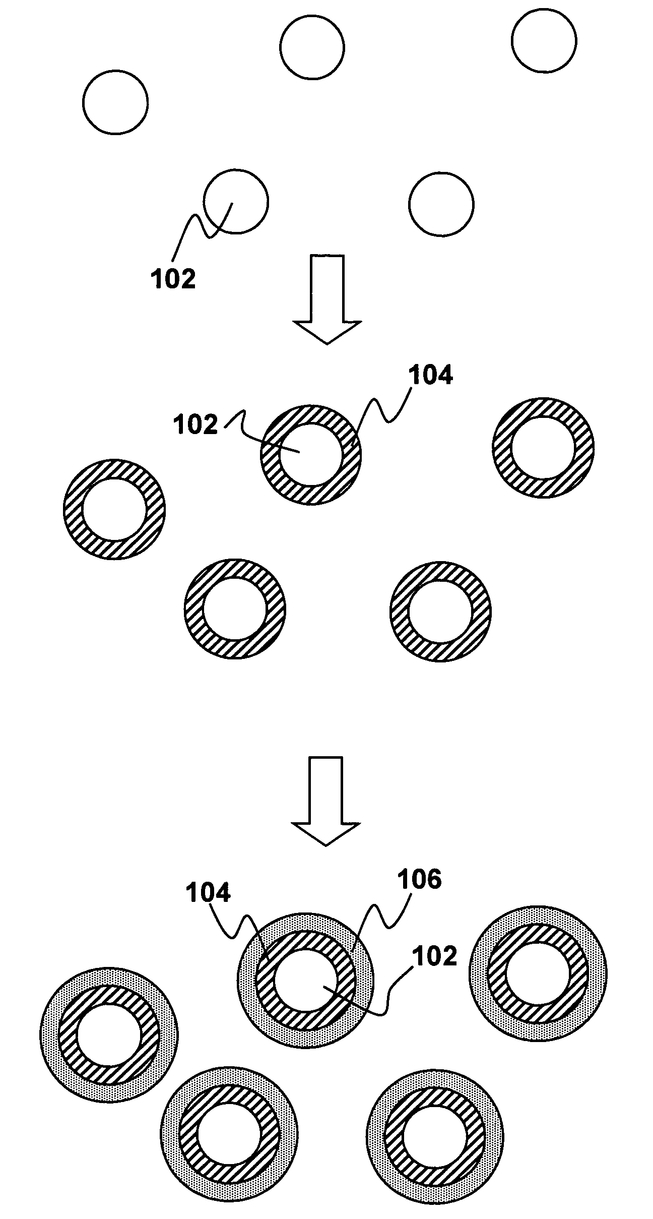
[0016]The disadvantages associated with the prior art may be overcome by fabricating CIGS absorber layers using coated nanoparticles. Nanoparticles are discrete entities sized less than about 1000 nm, more preferably less than about 500 nm, and still more preferably less than about 250 nm. When the nanoparticles are sized less than about 10 nm, their chemical, physical, electronic, and optical properties often change relative to that of bulk material, and at about the 10 nm or less size scale, nanoparticles are also called “quantum dots”.

[00...


PUM

PropertyMeasurementUnit
diameteraaaaaaaaaa
diameteraaaaaaaaaa
diameteraaaaaaaaaa

Abstract

CIGS absorber layers fabricated using coated semiconducting nanoparticles and / or quantum dots are disclosed. Core nanoparticles and / or quantum dots containing one or more elements from group IB and / or IIIA and / or VIA may be coated with one or more layers containing elements group IB, IIIA or VIA. Using nanoparticles with a defined surface area, a layer thickness could be tuned to give the proper stoichiometric ratio, and / or crystal phase, and / or size, and / or shape. The coated nanoparticles could then be placed in a dispersant for use as an ink, paste, or paint. By appropriate coating of the core nanoparticles, the resulting coated nanoparticles can have the desired elements intermixed within the size scale of the nanoparticle, while the phase can be controlled by tuning the stochiometry, and the stoichiometry of the coated nanoparticle may be tuned by controlling the thickness of the coating(s).

Description

FIELD OF THE INVENTION[0001]This invention is related to photovoltaic cells and more particularly to fabrication of IB-IIIA-VIA active layers for such cells.BACKGROUND OF THE INVENTION[0002]Low-cost production of solar cells on flexible substrates using printing or web coating technologies is promising a highly cost-efficient alternative to traditional silicon-based solar cells. Recently, solar cells with absorber layers fabricated by solution-based deposition of alloys of copper (Cu) and indium (In) with selenium (Se) or sulfur (S) have been developed. Such solar cells, generally referred to as CIGS cells, have been fabricated using different non-vacuum processes in which a precursor solution is formulated containing mixed oxides of Cu, In and Ga, which is then coated on a substrate. In particular, Kapur et al (U.S. Pat. No. 6,268,014, issued October 2000) describe a method for fabricating a solar cell based upon the solution-based deposition of a source material comprised of mecha...

Claims


Application Information

Patent Timeline
Patent Type & Authority Patents(United States)
IPC IPC(8): B05D5/12B05D1/36B05D7/00B22F1/054B22F1/17
CPCB22F1/0018B82Y20/00B82Y30/00C23C16/45544C23C18/1216C23C18/52H01L31/0322H01L31/035281H01L31/0384H01L31/0749H01L51/0026H01L51/426B22F1/025Y10T428/12181B22F2999/00H01L51/0037Y02E10/541Y10T428/2991Y02E10/549Y10S977/857Y10S977/89Y10S977/773Y10S977/892B22F1/02B22F2202/15B22F2202/01B22F1/054B22F1/17B22F1/056H10K71/40H10K85/1135H10K30/35B22F1/102
Inventor SAGER, BRIAN M.YU, DONGROBINSON, MATTHEW R.
Owner AERIS CAPITAL SUSTAINABLE IP
Why Eureka
Try Eureka