Method of forming package-on-package and device related thereto

a technology of semiconductor packages and packaging, applied in the field of semiconductor devices, can solve the problems of difficult stacking of semiconductor packages, and achieve the effect of reducing the width and height of the pop

Active Publication Date: 2012-10-23
SAMSUNG ELECTRONICS CO LTD
View PDF15 Cites 59 Cited by
  • Summary
  • Abstract
  • Description
  • Claims
  • Application Information

AI Technical Summary

Benefits of technology

[0006]Example embodiments of the inventive concepts provide a method of forming a package-on-package (PoP) capable of easily reducing the width and height of the PoP.

Problems solved by technology

However, it is very difficult to stack the plurality of semiconductor packages while controlling the width and height of the PoP.

Method used


Image

  • Method of forming package-on-package and device related thereto
  • Method of forming package-on-package and device related thereto
  • Method of forming package-on-package and device related thereto

Examples


first embodiment

[First Embodiment]

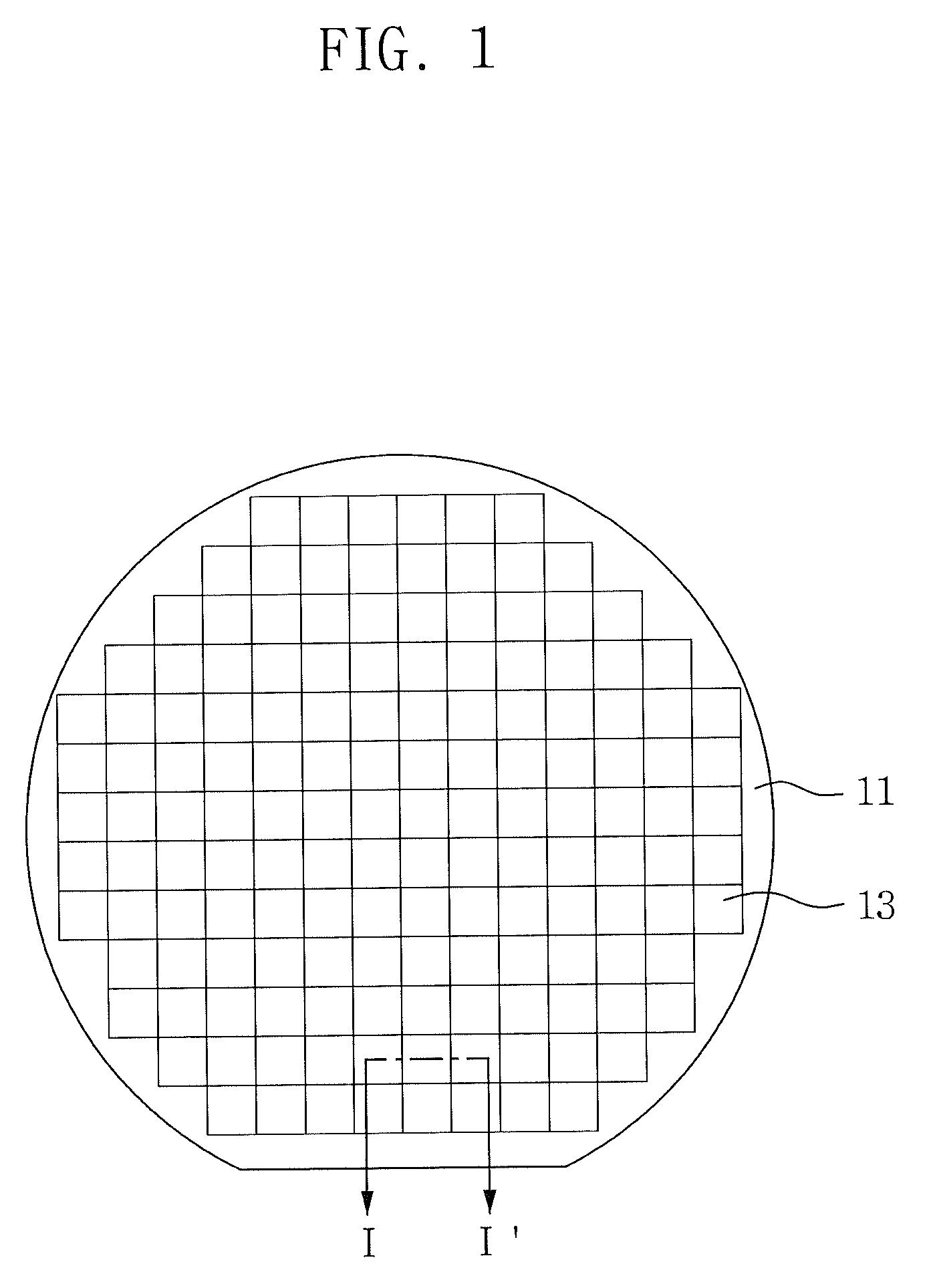
[0050]FIG. 1 is a plan view illustrating a method of forming a POP in accordance with a first example embodiment of the inventive concepts, and FIGS. 2 to 13 are cross-sectional views illustrating the method of forming a PoP in accordance with the first example embodiment of the inventive concepts. Here, FIGS. 2 to 6 and 8 are cross-sectional views taken along line I-I′ of FIG. 1, and FIG. 7A is an enlarged view of a portion K of FIG. 6.

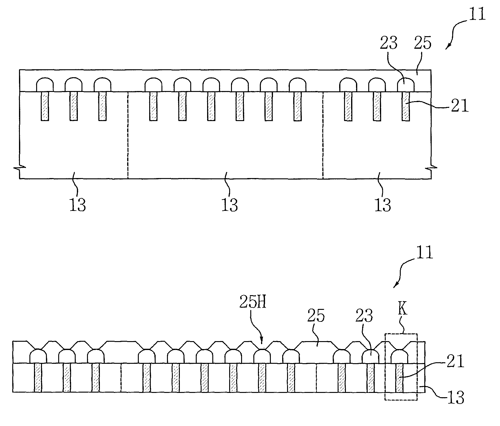
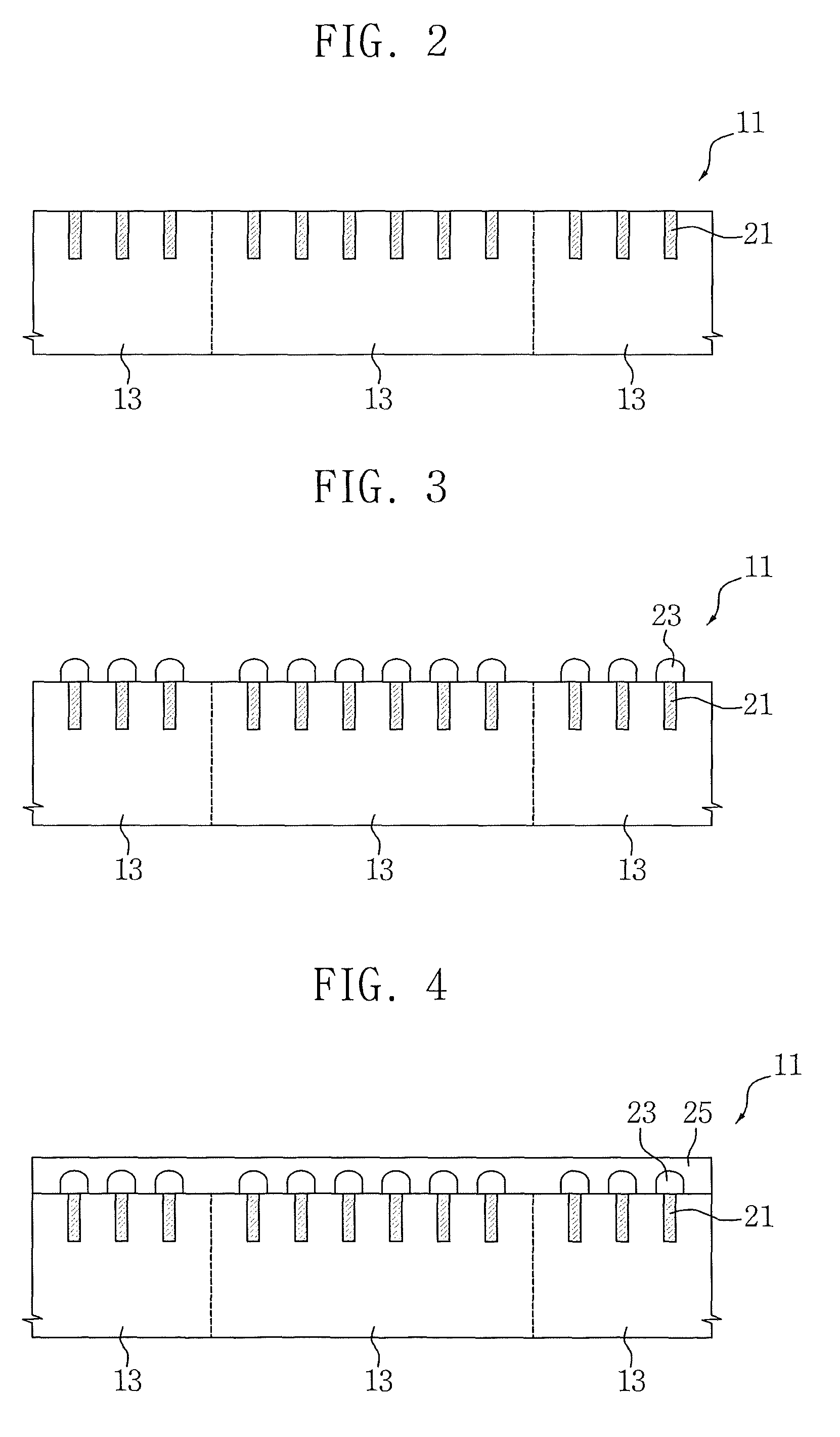
[0051]Referring to FIGS. 1 and 2, the method of forming a PoP in accordance with the first example embodiment of the inventive concepts may include forming a plurality of through silicon vias (TSVs) 21 on a wafer 11. The wafer 11 may include a plurality of semiconductor chips 13. The semiconductor chips 13 may be disposed in a two-dimensional array having rows and columns.

[0052]The TSVs 21 may be a conductive layer formed of at least one selected from the group consisting of tungsten (W), tungsten nitride (WN), titanium (Ti), titani...

second embodiment

[Second Embodiment]

[0089]FIGS. 14 to 20 are cross-sectional views illustrating a method of forming a PoP in accordance with a second example embodiment of the inventive concepts.

[0090]Referring to FIG. 14, the method of forming a PoP in accordance with a second example embodiment of the inventive concepts may include forming a plurality of TSVs 21 in a wafer 11. The wafer 11 may include a plurality of semiconductor chips 13. The TSVs 21 may be formed to penetrate the wafer 11 from one surface to a depth that may or may not be predetermined.

[0091]An encapsulant 25 may be formed on the wafer 11 using a wafer level molding process. The encapsulant 25 may cover the TSVs 21. The encapsulant 25 may be formed of EMC containing resin and filler. In some embodiments, the encapsulant 25 may be fanned using liquid resin such as an underfill.

[0092]Referring to FIG. 15, the wafer 11 may be partially removed to expose the TSVs 21. For example, a lower surface of the wafer 11 may be partially remo...

third embodiment

[Third Embodiment]

[0105]FIGS. 21 and 22 are cross-sectional views illustrating a method of forming a PoP in accordance with a third example embodiment of the inventive concepts.

[0106]Referring to FIG. 21, the method of forming a PoP in accordance with the third example embodiment of the inventive concepts may include forming a plurality of TSVs 21 on a wafer 11. The wafer 11 may include a plurality of semiconductor chips 13. The wafer 11 may be partially removed to expose the TSVs 21. For example, a lower surface of the wafer 11 may be partially removed using a CMP process, an etch-back process, a back grinding process, and / or a combination thereof, until one ends of the TSVs 21 are exposed. As a result, the thickness of the wafer 11 can be remarkably reduced. One ends of the TSVs 21 may be exposed by one surface of the wafer 11, and the other ends of the TSVs 21 may be exposed by the other surface of the wafer 11.

[0107]Referring to FIG. 22, internal connection terminals 23 may be f...


PUM


Abstract

Provided is a method of forming a package-on-package. An encapsulation is formed to cover a wafer using a wafer level molding process. The wafer includes a plurality of semiconductor chips and a plurality of through silicon vias (TSVs) passing through the semiconductor chips. The encapsulant may have openings aligned with the TSVs. The encapsulant and the semiconductor chips are divided to form a plurality of semiconductor packages. Another semiconductor package is stacked on one selected from the semiconductor packages. The other semiconductor package is electrically connected to the TSVs.

Description

CROSS-REFERENCE TO RELATED APPLICATION[0001]This application claims priority under 35 U.S.C. §119 to Korean Patent Application No. 10-2010-26393 filed on Mar. 24, 2010, in the Korean Intellectual Property Office (KIPO), the disclosure of which is hereby incorporated by reference in its entirety.BACKGROUND[0002]1. Field[0003]Example embodiments of the inventive concepts relate to a semiconductor device and a method of forming the same, and more particularly, to a method of forming a package-on-package and a device related thereto.[0004]2. Description of Related Art[0005]As electronic devices have become thinner and smaller-sized, techniques related to a package-on-package (PoP) have been widely researched. The PoP refers to a package in which the same or different kinds of semiconductor packages are stacked to reduce a horizontal mounting surface, increasing the degree of integration thereof. However, it is very difficult to stack the plurality of semiconductor packages while control...

Claims


Application Information

Patent Timeline
Patent Type & Authority Patents(United States)
IPC IPC(8): H01L21/00H01L23/02
CPCH01L25/16H01L25/105H01L23/5226H01L25/50H01L25/0657H01L21/78H01L23/481H01L24/14H01L23/3128H01L2224/48225H01L2225/1058H01L2924/01019H01L2224/45124H01L2224/45144H01L2225/1052H01L2224/94H01L2224/16225H01L2224/16145H01L2224/14181H01L2225/1005H01L2924/10253H01L24/81H01L24/97H01L2924/00H01L2224/11H01L2224/48227H01L2924/12042H01L2924/181H01L2224/13022H01L2224/13025H01L2224/16146H01L2224/17181H01L2224/32145H01L2224/32225H01L2224/73204H01L2225/1023H01L2924/15311H01L2924/15331H01L2225/06541H01L2225/06565H01L2924/00012
Inventor KIM, TAE-HUNPARK, JIN-WOOCHOI, DAE-YOUNGKIM, MI-YEONLEE, SUN-HYE
Owner SAMSUNG ELECTRONICS CO LTD
Why Eureka
Try Eureka