On-wafer butted microbolometer imaging array

a microbolometer and imaging array technology, applied in the field of night vision devices, can solve the problems of unacceptably low yield and high cost, low reticle yields, and large investment loss, and achieve the effect of better imaging

a microbolometer and imaging array technology, applied in the field of night vision devices, can solve the problems of unacceptably low yield and high cost, low reticle yields, and large investment loss, and achieve the effect of better imaging

US8294099B2Active Publication Date: 2012-10-23BAE SYST INFORMATION & ELECTRONICS SYST INTEGRATION INC

Image

  • On-wafer butted microbolometer imaging array
  • On-wafer butted microbolometer imaging array
  • On-wafer butted microbolometer imaging array

Examples


Embodiment Construction

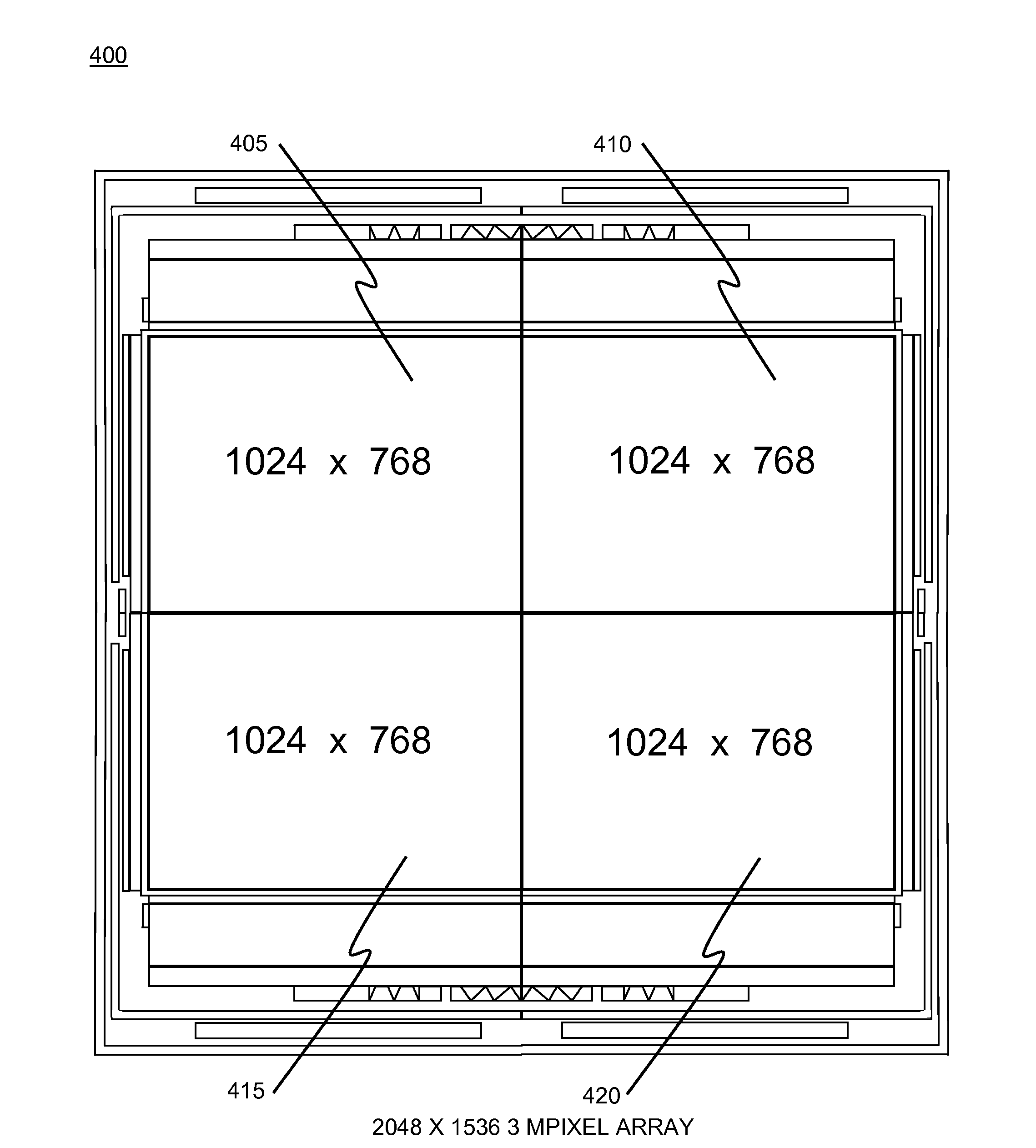
[0026]An advantage of on-wafer buttable array imaging systems is that they achieve higher effective frame rates than a fully-scaled imaging array. In on-wafer buttable system embodiments, each component FPA runs at the frame rate typical of that size array. Additionally, the on-wafer buttable approach avoids the difficult very large scaled FPA ROIC design required to maintain the frame rate of very large scaled FPAs as the number of pixels is increased.

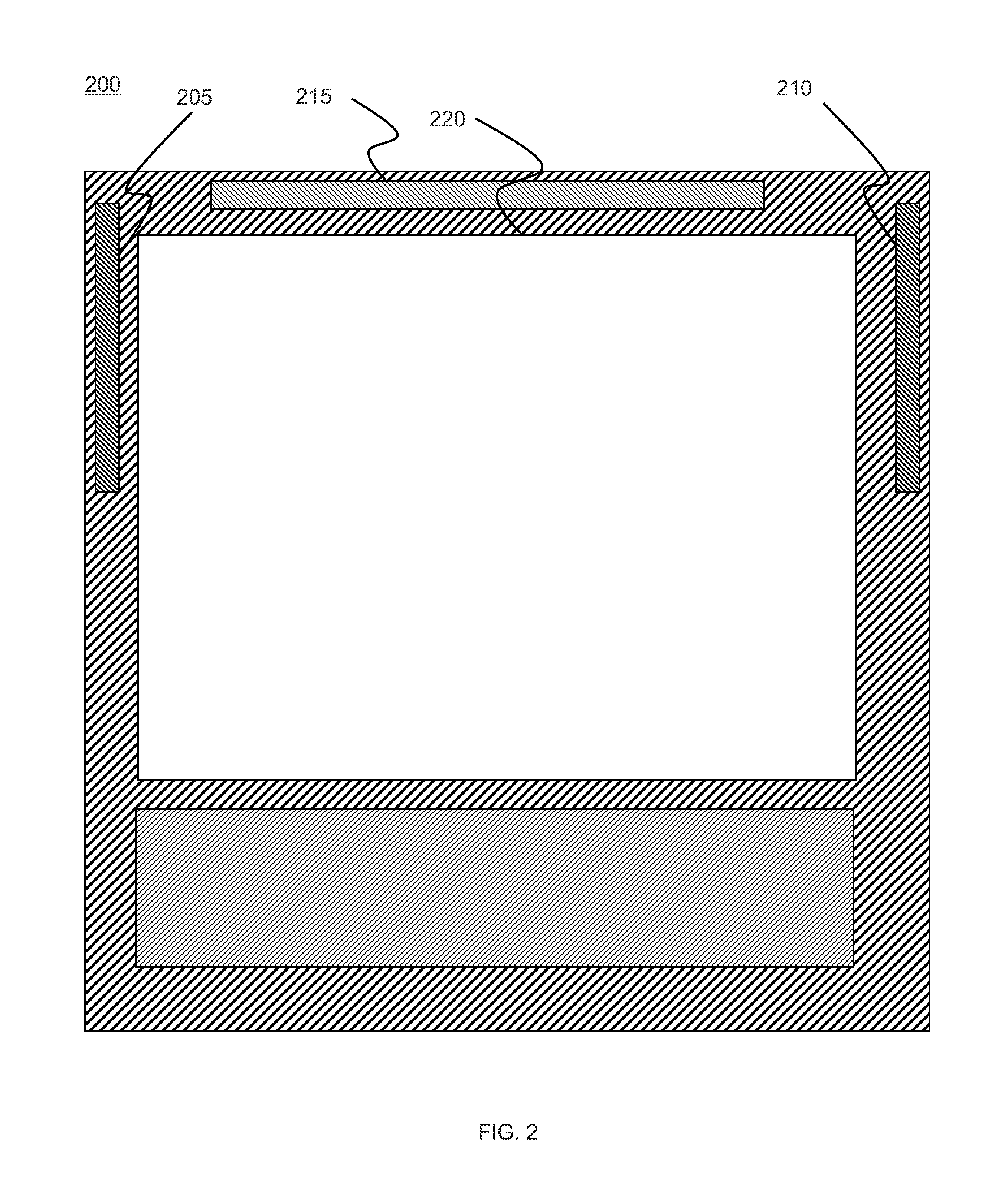
[0027]The ROIC / FPA modifications require only layout changes rather than actual circuit changes and are low risk projects. The types of layout changes needed for buttable FPAs are evident from the floor plan plot 200 in FIG. 2.

[0028]The strips along each of the left 205, right 210, and top 215 edges of the chip are the bond pad areas. For embodiments, the top and left sides are devoid of bond pads and provide for on-wafer seamless butting. In embodiments, a modest amount of circuitry along the top and left side of the pixel array is r...


PUM

PropertyMeasurementUnit
sizeaaaaaaaaaa
gap dimensionaaaaaaaaaa
infrared imagingaaaaaaaaaa

Abstract

An apparatus and method for assembling a large microbolometer infrared imaging array from sub-arrays, including the step of forming a sub-array assembly of independent imaging arrays on the silicon wafer as the imaging sensor is being processed, whereby seams or gaps in a resulting image are avoided.

Description

RELATED APPLICATIONS[0001]This application claims the benefit of U.S. Provisional Application Ser. No. 61 / 168,274 filed 10 Apr. 2009, herein incorporated in its entirety by reference.FIELD OF THE INVENTION[0002]The present invention relates to night vision devices and more particularly to microbolometer imaging arrays.BACKGROUND OF THE INVENTION[0003]The need for very large uncooled imaging systems has outpaced the development of large format focal plane arrays (FPAs). This need has motivated approaches to build very large uncooled imaging arrays using smaller arrays mechanically-butted together to form a larger imaging system. Smaller FPAs can be mechanically assembled in close proximity on a common carrier to form a larger imaging array.[0004]Another approach to large format FPAs is reticle stitching. Reticle stitching is directed to producing larger FPAs by sub-dividing a circuitry pattern and then stitching, or recomposing the subfield patterns together using one or more reticle...

Claims


Application Information

Patent Timeline
23 Oct 2012
Publication
US8294099B2
IPC
G01J5/00
CPC
H01L27/14618; Y10T29/4913; H01L2924/0002; H01L2924/00
Inventors
BLACKWELL, JR., RICHARD J.