Semiconductor device comprising transistor having gate and drain connected through a current-voltage conversion element

a current-voltage conversion element and semiconductor technology, applied in static indicating devices, instruments, electroluminescent light sources, etc., can solve the problem of inability to perform accurate display, suppress an increase in manufacturing costs, reduce the off current flowing to a rectifying element or a transistor, and improve yield

Inactive Publication Date: 2012-10-30
SEMICON ENERGY LAB CO LTD
View PDF36 Cites 26 Cited by
  • Summary
  • Abstract
  • Description
  • Claims
  • Application Information

AI Technical Summary

Benefits of technology

[0032]In view of this, the invention provides a display device which suppresses an increase in manufacturing cost and improves yield.
[0043]A switch used in the invention may be any switch such as an electrical switch or a mechanical switch. That is, it may be anything as far as it can control a current and is not limited to a particular type. It may be a transistor, a diode (PN diode, PIN diode, Schottky diode, diode-connected transistor, and the like), or a logic circuit configured with them. Therefore, in the case of applying a transistor as a switch, polarity (conductivity) thereof is not particularly limited because it operates just as a switch. However, when an off current is preferred to be small, a transistor of polarity with a small off current is favorably used. For example, the transistor which has an LDD region or a multi-gate structure has a small off current. Further, it is desirable that an N-channel transistor is employed when a potential of a source terminal of the transistor as a switch is closer to the low potential side power source (Vss, GND, 0 V and the like), and a P-channel transistor is desirably employed when the potential of the source terminal is closer to the high potential side power source (Vdd and the like). This helps the switch operate efficiently as the absolute value of the gate-source voltage of the transistor can be increased. It is also to be noted that a CMOS switch can also be applied by using both N-channel and P-channel transistors. With a CMOS switch, an operation can be appropriately performed even when the situation changes such that a voltage outputted through a switch (that is, an input voltage) is higher or lower than an output voltage.
[0047]It is to be noted that various types of transistors can be used as a transistor of the invention and formed over various substrates. Therefore, all of the circuits may be formed over a glass substrate, a plastic substrate, a single crystal substrate, an SOI substrate, or any substrate. When all the circuits are formed over a substrate, cost can be reduced by reducing the number of components and reliability can be improved by reducing the number of connections with the components. Alternatively, a part of a circuit may be formed over a certain substrate and another part of the circuit may be formed over another substrate. That is, not all of the circuits is required to be formed over the same substrate. For example, a part of a circuit may be formed over a glass substrate using a transistor and another part of the circuit may be formed over a single crystal substrate into an IC chip which may be provided over the glass substrate by COG (Chip On Glass). Alternatively, the IC chip may be connected to a glass substrate using TAB (Tape Automated Bonding) or a printed substrate. In this manner, when parts of a circuit are formed over the same substrate, cost can be reduced by reducing the number of components and reliability can be improved by reducing the number of connections with the components. Further, a portion with a high driving voltage or a high driving frequency which consumes more power is not preferably formed over the same substrate, thereby an increase in power consumption can be prevented.
[0048]It is to be noted that a transistor can have structures of various modes and is not limited to a specific structure. For example, a multi-gate structure which has two or more gate lines may be employed as well. With a multi-gate structure, an off current can be reduced and reliability can be improved by improving the pressure resistance of a transistor, and further flat characteristics can be obtained that a drain-source current hardly changes even when a drain-source voltage changes in the operation in a saturation region. Further, gate electrodes may be provided over and under a channel. Accordingly, a channel region increases, thereby an S value (sub-threshold coefficient) can be improved since a current value is easily increased and a depletion layer is easily formed. Further, a gate electrode may be provided over a channel or under the channel. A forward staggered structure or an inversely staggered structure may be employed. A channel region may be divided into a plurality of regions, connected in parallel, or connected in series. Further, a source electrode or a drain electrode may overlap a channel (or a part of it). Accordingly, a charge is accumulated in a part of the channel and an unstable operation can be prevented. Further, an LDD region may be provided. By providing an LDD region, an off current can be reduced and reliability can be improved by improving the pressure resistance of a transistor, and further flat characteristics can be obtained that a drain-source current hardly changes even when a drain-source voltage changes in the operation in a saturation region.
[0065]According to the invention, an off current flowing to a rectifying element or a transistor can be reduced. Therefore, it can be prevented that a light emitting element of a pixel to which a signal for non-light emission (black display) is inputted slightly emits light.
[0066]Further, a display device can be provided which can suppress an increase in manufacturing cost and improve the yield to reduce an off current of a transistor or a rectifying element without increasing the manufacturing steps.

Problems solved by technology

Then, an accurate display cannot be performed.

Method used


Image

  • Semiconductor device comprising transistor having gate and drain connected through a current-voltage conversion element
  • Semiconductor device comprising transistor having gate and drain connected through a current-voltage conversion element
  • Semiconductor device comprising transistor having gate and drain connected through a current-voltage conversion element

Examples


embodiment mode 1

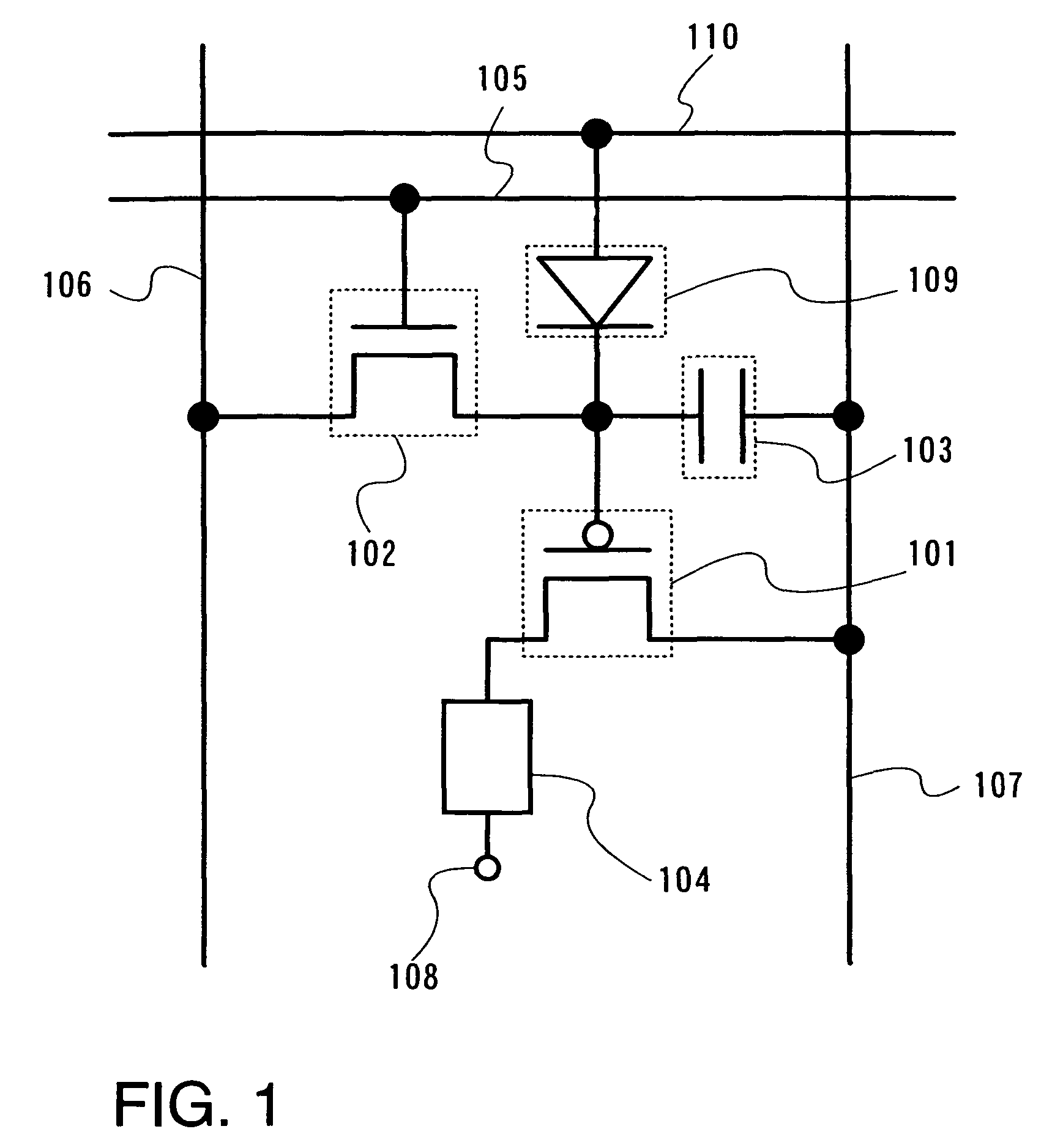
[0138]In this embodiment mode, description is made on a pixel configuration in the case of applying a rectifying element as a potential transfer unit and to a display device having the pixel.

[0139]First, description is made with reference to FIG. 1 on a basic pixel configuration of this embodiment mode. Here, only one pixel is shown, but a plurality of pixels are arranged in matrix of the row direction and the column direction in a pixel portion of a display device.

[0140]The pixel shown in FIG. 1 includes a driving transistor 101, a switching transistor 102, a capacitor 103, a light emitting element 104, a first scan line 105, a signal line 106, a power source line 107, a rectifying element 109, and a second scan line 110. It is to be noted that the driving transistor 101 is a P-channel transistor and the switching transistor 102 is an N-channel transistor. The switching transistor 102 has a gate terminal connected to the first scan line 105, a first terminal (source terminal or dra...

embodiment mode 2

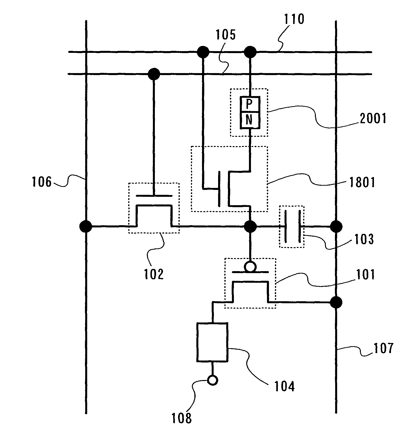
[0210]In this embodiment mode, description is made on a configuration where a circuit element having three terminals is used as a potential transfer unit.

[0211]First, description is made with reference to FIG. 53 on a basic pixel configuration of this embodiment mode. In the pixel, a transistor 5301, a switch 5302, a potential holding element 5303, a light emitting element 5304, a first scan line 5305, a signal line 5306, a power source line 5307, a second scan line 5310, and a potential transfer element 5309 are provided. The switch 5302 is connected to control the conduction or no conduction between the signal line 5306 and a gate terminal of the transistor 5301. Further, a control terminal of the switch 5302 is connected to the first scan line 5305. Accordingly, the switch 5302 is turned on / off depending on a signal inputted to the first scan line 5305, thereby controlling the conduction or no conduction between the signal line 5306 and the gate terminal of the transistor 5301. M...

embodiment mode 3

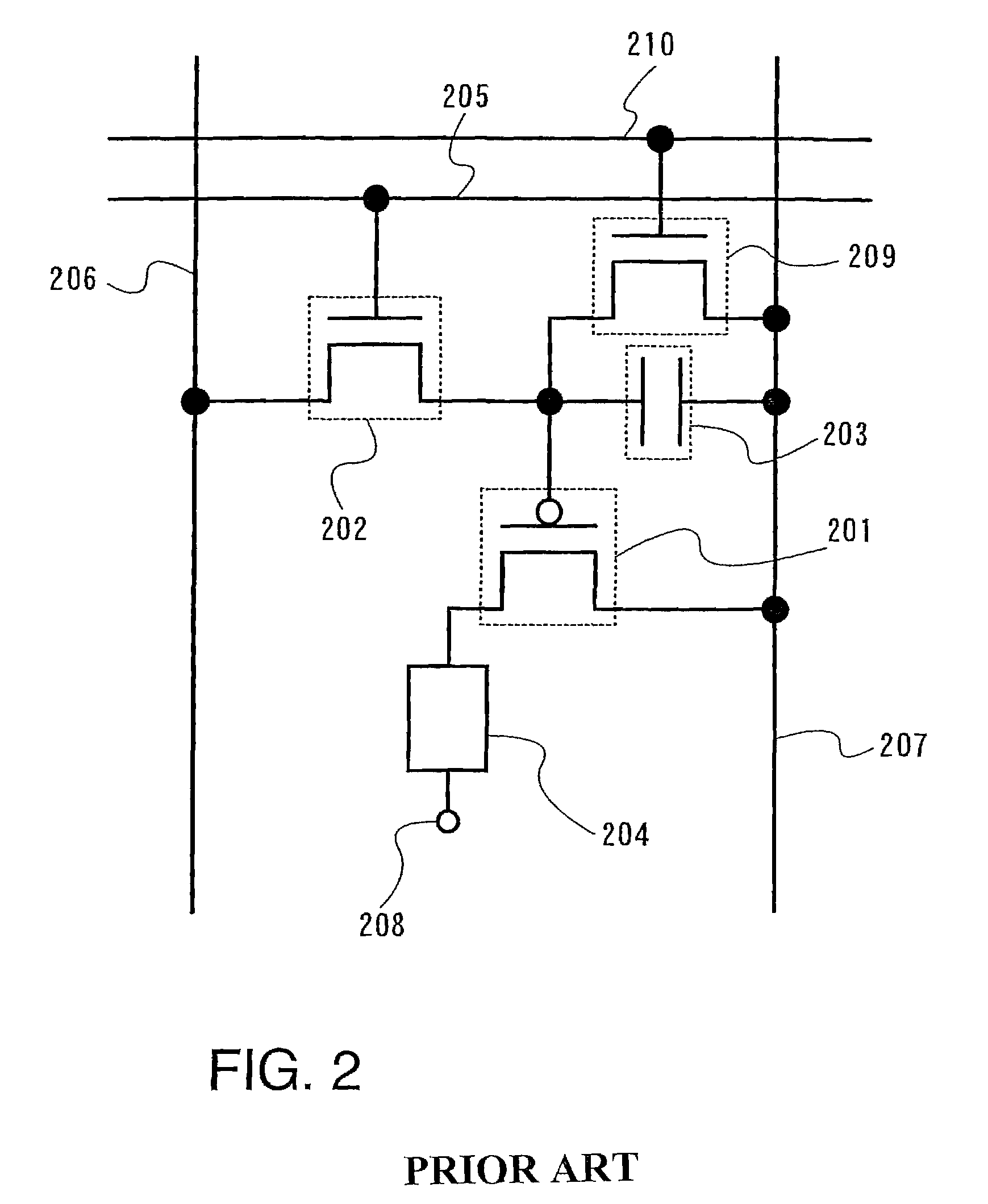
[0295]In this embodiment mode, a pixel configuration is shown which can further prevent that a light emitting element slightly emits light when the pixel is required to emit no light (black display). That is, when an off current flows through a driving transistor, the current is prevented from flowing to a light emitting element.

[0296]In a pixel shown in FIG. 56, a driving transistor 5601, a complementary transistor 5611, a switching transistor 5602, a light emitting element 5604, a rectifying element 5609, a first scan line 5605, a signal line 5606, a power source line 5607, and a second scan line 5610 are provided. It is to be noted that the driving transistor 5601 is a P-channel transistor, and the complementary transistor 5611 and the switching transistor 5602 are N-channel transistors. A first terminal (source terminal or drain terminal) of the switching transistor 5602 is connected to the signal line 5606 and a second terminal (source terminal or drain terminal) thereof is con...


PUM


Abstract

When a signal inputted to a pixel is erased by setting potentials of a gate terminal and a source terminal of a driving transistor to be equal, a current slightly flows through the driving transistor in some cases, which leads to occur a display defect. The invention provides a display device which improves the yield while suppressing the increase in manufacturing cost. When a potential of a scan line for erasure is raised, a potential of the gate terminal of the driving transistor is raised accordingly. For example, the scan line and the gate terminal of the driving transistor are connected through a rectifying element.

Description

BACKGROUND OF THE INVENTION[0001]1. Field of the Invention[0002]The invention relates to a semiconductor device having a function to control with a transistor a current supplied to a load. In particular, the invention relates to a pixel formed of a current drive type light emitting element of which luminance changes by a current, to a display device including a scan line driver circuit and a signal line driver circuit, and to a driving method thereof. Further, the invention relates to an electronic device having the display device in the display portion.[0003]2. Description of the Related Art[0004]In recent years, what is called a self-luminous type display device, which has pixels formed of light emitting elements such as light emitting diodes (LEDs), is attracting attentions. As a light emitting element used for such a self-luminous type display device, an organic light emitting diode (OLED), an organic EL element, and electroluminescence (also referred to as an electroluminescenc...

Claims


Application Information

Patent Timeline
Patent Type & Authority Patents(United States)
IPC IPC(8): G06F3/038H05B44/00
CPCG09G3/20G09G3/3233G09G3/2022G09G3/30G09G2300/0408G09G2300/0814G09G2330/08G09G2310/0251G09G2310/0262G09G2310/061G09G2320/0233G09G2330/04G09G2300/0847
Inventor KIMURA, HAJIME
Owner SEMICON ENERGY LAB CO LTD
Why Eureka
Try Eureka