Semiconductor device and method for manufacturing the same

a technology of semiconductor devices and semiconductors, applied in semiconductor devices, semiconductor/solid-state device details, electrical devices, etc., can solve the problems of increase in manufacturing costs, and deterioration in their respective performances, so as to suppress an increase in manufacturing costs and prevent deterioration in performan

Inactive Publication Date: 2015-10-08
SUKEKAWA MITSUNARI
View PDF5 Cites 12 Cited by
  • Summary
  • Abstract
  • Description
  • Claims
  • Application Information

AI Technical Summary

Benefits of technology

[0012]According to the present invention it is possible to prevent a deterioration in performance arising as a result of semiconducto

Problems solved by technology

With the progress of miniaturization, differences have arisen in the manufacturing processes for the respective regions, and thus if the regions are manufactured on the same wafer, there are problems in that semiconductor process constraints cause a deterioration in their respective performances, and the manufacturing cost also increases.
However, in the abovementioned first mode of embodiment the wiring lines from the memory cells to the sense amplifiers (SA) are long and are liable to affected by noise.
With the progress of miniaturization, differences have arisen in the manufacturing processes for the respective regions, and thus if the regions are manufactured on the same wafer, there are problems in that semiconductor process constraints cause a deterioration

Method used


Image

  • Semiconductor device and method for manufacturing the same
  • Semiconductor device and method for manufacturing the same
  • Semiconductor device and method for manufacturing the same

Examples


Embodiment Construction

Related Art

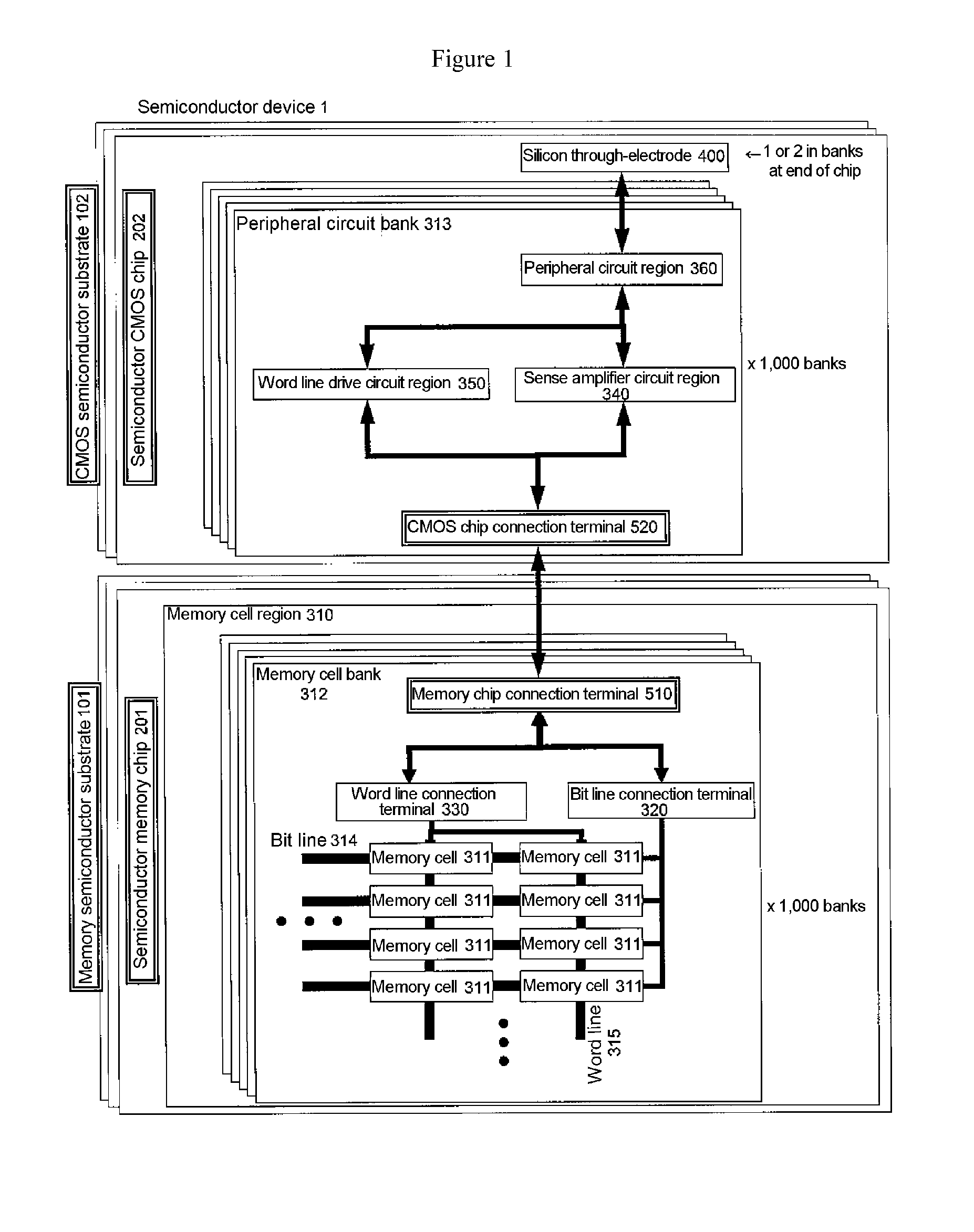
[0073]A semiconductor device (DRAM) according to the related art will first be described with reference to FIG. 10, in order to clarify the characteristics of the present invention. FIG. 10 is a drawing illustrating the structure of a semiconductor device according to the related art.

[0074]FIG. 10 (a) is a block connection diagram of circuit regions in a DRAM semiconductor device 1 in the related art.

[0075]Peripheral circuit regions (referred to collectively as a peripheral circuit region 360) excluding a sense amplifier circuit region 340 and a word line drive circuit region 350 are disposed abutting and electrically connecting the sense amplifier region 340 and the word line drive circuit region 350. A portion of the peripheral circuit region 360 exchanges signals with the outside.

[0076]FIG. 10 (b) is a cross-sectional view of the DRAM semiconductor device 1 in the related art.

[0077]A memory cell region 310, the sense amplifier circuit region 340, the word line drive ci...


PUM


Abstract

A semiconductor device comprising: a first semiconductor chip provided with a first function, including a memory element but not including a peripheral circuit; first connection terminals provided in the first semiconductor chip; a second semiconductor chip provided with a second function, including a peripheral circuit but not including a memory element; and second connection terminals provided in the second semiconductor chip, wherein the first semiconductor chip and the second semiconductor chip are stacked on one another by causing the first connection terminals and the second connection terminals to come into contact with one another.

Description

TECHNICAL FIELD[0001]The present invention relates to a semiconductor device and a method for manufacturing the same.BACKGROUND ART[0002]Generally, a DRAM (Dynamic Random Access Memory) comprises a memory cell region (generally formed as an NMOS) having a capacitor structure, and a peripheral circuit region comprising CMOS circuits. With the progress of miniaturization, differences have arisen in the manufacturing processes for the respective regions, and thus if the regions are manufactured on the same wafer, there are sometimes problems in that semiconductor process constraints cause a deterioration in their respective performances, and the manufacturing cost also increases.[0003]Examples of the related art are described in JP2011-228484 (patent literature 1), JP2006-319243 (patent literature 2) and JP2008-16720 (patent literature 3).[0004]Patent literature 1 discloses stacking a DRAM core chip and an interface chip on one another, and electrically connecting them using through-el...

Claims


Application Information

Patent Timeline
IPC IPC(8): H01L25/18H01L27/108H01L23/532H01L23/528H01L27/088H01L23/48H01L25/065H01L23/544
CPCH01L25/18H01L25/0657H01L27/10805H01L23/544H01L2223/54426H01L27/088H01L23/481H01L23/53228H01L2225/06541H01L23/528H01L2924/0002H01L23/642H01L2225/06513H01L2223/54453H01L2223/5446H10B12/50H01L2924/00H10B12/30
Inventor SUKEKAWA, MITSUNARI
Owner SUKEKAWA MITSUNARI
Why Eureka
Try Eureka