Three-dimensional semiconductor structure

a three-dimensional, resistive random access memory technology, applied in semiconductor devices, digital storage, instruments, etc., can solve the problems of limiting the total size and applications of the memory, limiting the speed, the number, and the retention of the contents of the rom, so as to achieve a simple and low-cost method

Active Publication Date: 2012-11-06
MACRONIX INT CO LTD
View PDF3 Cites 3 Cited by
  • Summary
  • Abstract
  • Description
  • Claims
  • Application Information

AI Technical Summary

Benefits of technology

[0011]It is therefore an object of the present invention to provide a three-dimensional (3D) semiconductor device, especially a high-density 3D resistive random-access memory (RRAM) structure, fabricated by a simple and low-cost method.

Problems solved by technology

ROM retains the contents even in the absence of power, but is limited in the speed, the number of times to which it may be written, and the manner in which it may be written.
However, its volatility (i.e. it will lose its contents when the power is switched off), large size and stand-by current limit the total size and applications of the memory.
DRAM has the smallest cell size, but necessitates a complex refresh algorithm, and is also necessary to supply voltage at all times or the information will disappear (i.e. volatile).

Method used


Image

  • Three-dimensional semiconductor structure
  • Three-dimensional semiconductor structure
  • Three-dimensional semiconductor structure

Examples


first embodiment

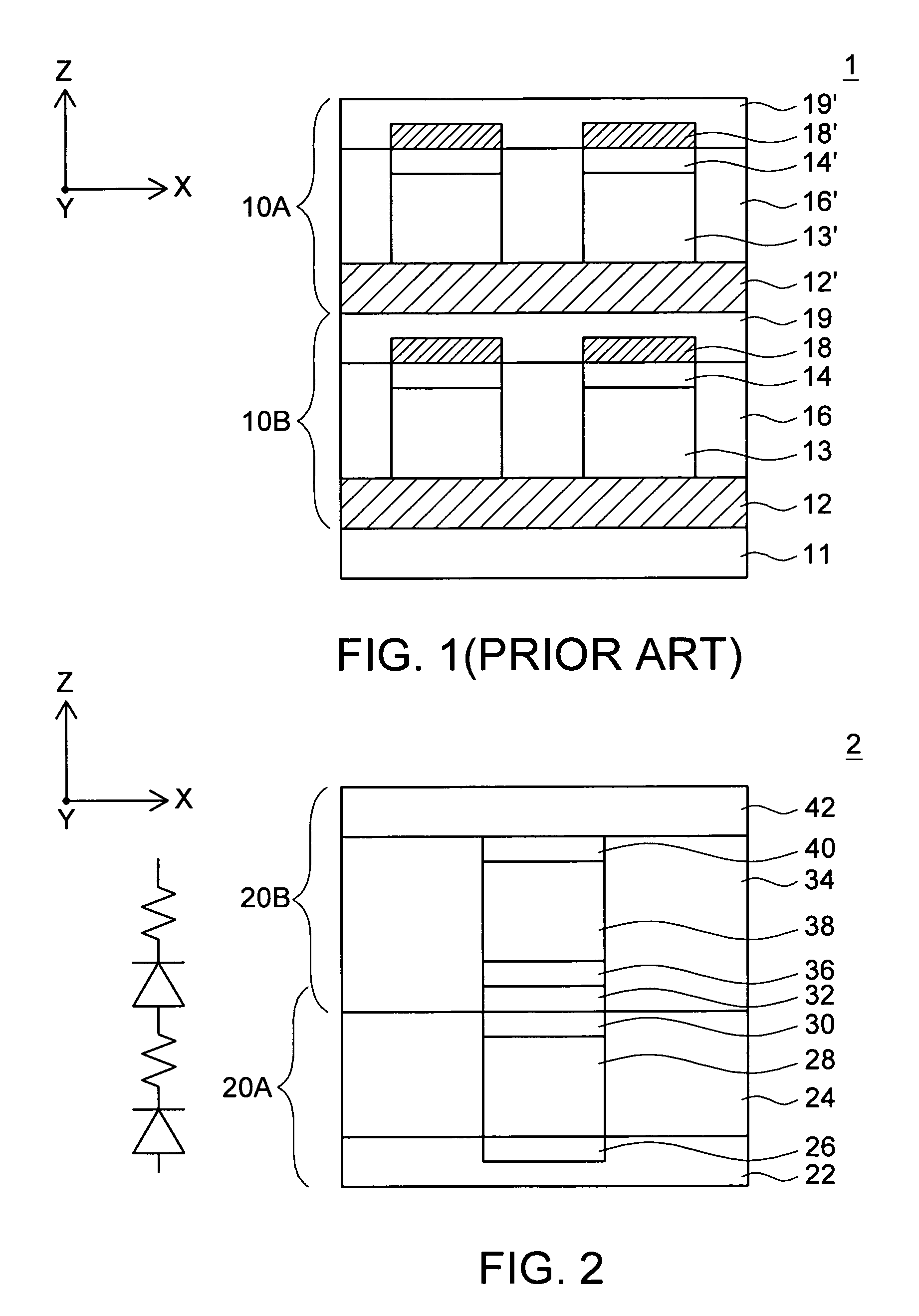
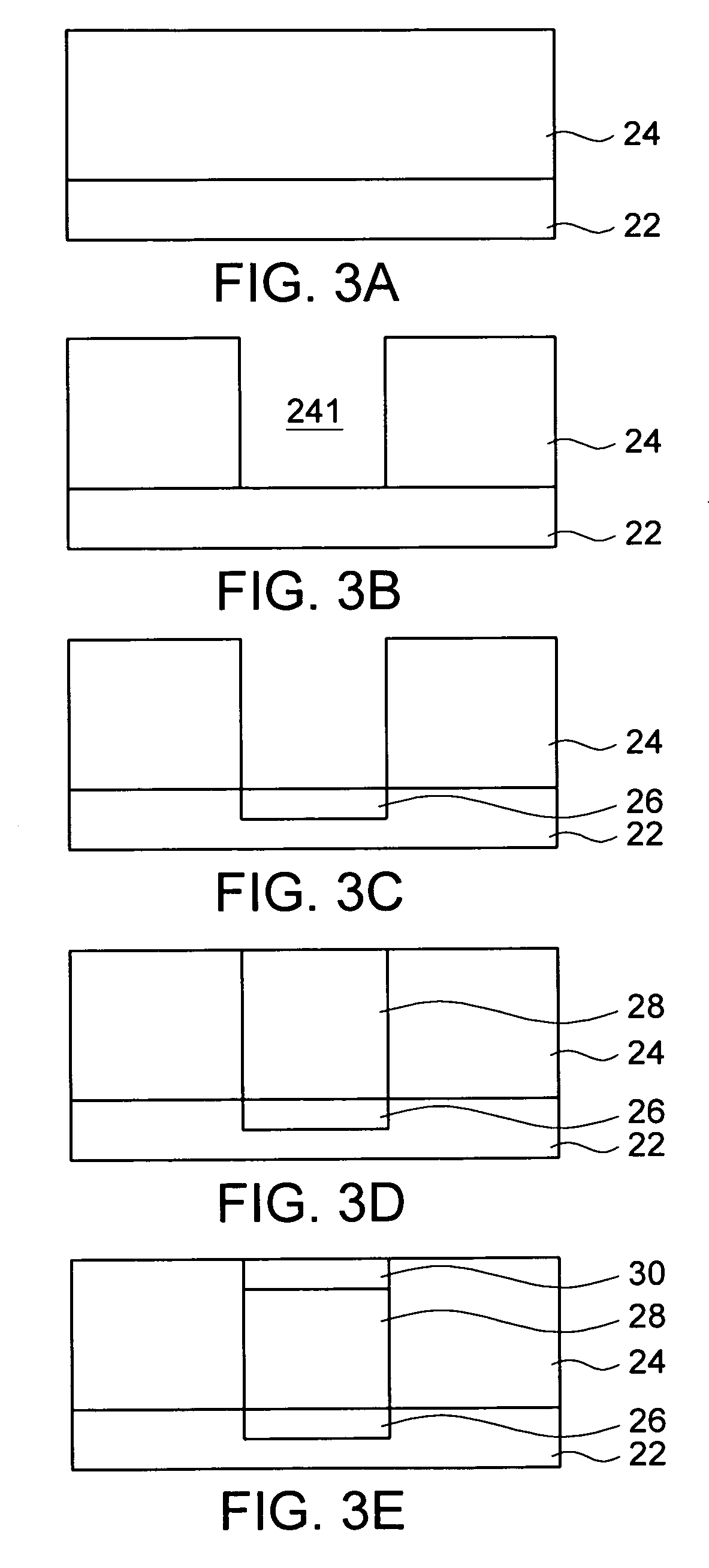
[0027]FIG. 2 schematically shows a cross-sectional view of a three-dimensional (3D) semiconductor structure according to the first embodiment of the present invention. As shown in FIG. 2, the 3D semiconductor structure 2 is constructed by vertically stacking at least two memory cells 20A and 20B, and the second memory cell 20B is stacked on the first memory cell 20A. The first memory cell 20A could be supported by a base layer (not shown) made of insulation material. Alternatively, the base layer is formed on a substrate (not shown), in which the base layer and the substrate support the 3D semiconductor structure 2.

[0028]The first memory cell 20A includes a first conductive line 22, a first doped region 26, a first metal layer 28, a first metal oxide layer 30, and a second conductive line 32 opposite to the first conductive line 22. The first conductive line 22 and the second conductive line 32 could be the P-type conductive lines. The first doped region 26, such as a N-doped region...

second embodiment

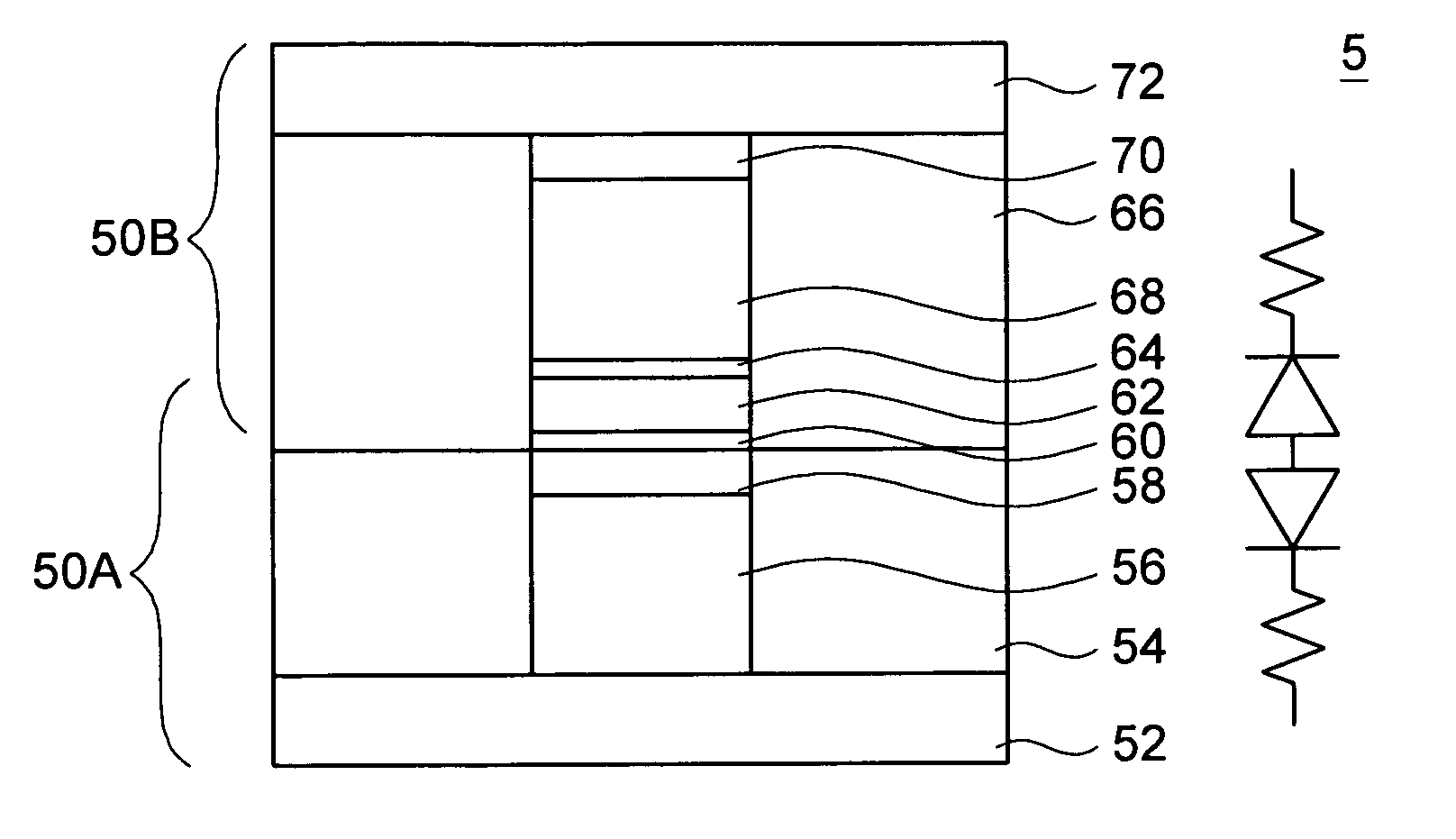
[0044]FIG. 4 schematically shows a cross-sectional view of a three-dimensional (3D) semiconductor structure according to the second embodiment of the present invention. As shown in FIG. 4, the 3D semiconductor structure 5 is constructed by vertically stacking at least two memory cells 50A and 50B. The structures of the first and second embodiments are similar, except the positions of the diode elements are slightly modified in the first and second memory cells 50A and 50B.

[0045]As shown in FIG. 4, the first memory cell 50A includes a first conductive line 52, a first metal layer 56, a first metal oxide layer 58, a first doped region 60, and a second conductive line 62 opposite to the first conductive line 52. The first conductive line 52 and the second conductive line 62 could be the P-type conductive lines. The first metal layer 56 is formed on the first conductive line 52, and the first metal oxide layer 58 is formed on the first metal layer 56. The first doped region 60, such as ...

third embodiment

[0058]FIG. 6 schematically shows a cross-sectional view of a three-dimensional (3D) semiconductor structure according to the third embodiment of the present invention. The 3D semiconductor structure 6 of the third embodiment is similar to the 3D semiconductor structure 2 of the first embodiment, except that each memory cell of the third embodiment includes plural memory elements so as to fabricate a 3D semiconductor structure with multi-level cells (MLC, i.e. each memory cell capable of storing a plurality of bits). The elements of FIG. 6 identical to the elements of FIG. 2 are designated with the same reference numbers. Also, the method of fabricating the semiconductor structure 6 of the third embodiment could be referred to the description in the first embodiment.

[0059]According to the 3D semiconductor structure 6 of the third embodiment (FIG. 6), the first memory cell 60A comprises at least two memory elements (i.e. two multi-layer units), including a first multi-layer unit 281 (...


PUM


Abstract

A three-dimensional (3D) semiconductor structure with high density and method of fabricating the same are disclosed. The 3D semiconductor structure comprises at least a first memory cell and a second memory cell stacked on the first memory cell. The first memory cell comprises a first conductive line and a second conductive line. The second memory cell comprises another first conductive line opposite to the first conductive line of the first memory cell, and the second conductive line formed between said two first conductive lines of the first and second memory cells. The first and second memory cells share the second conductive line when the 3D semiconductor structure is programming and erasing, and each of the first and second memory cells has a diode.

Description

BACKGROUND OF THE INVENTION[0001]1. Field of the Invention[0002]The invention relates in general to a three-dimensional (3D) semiconductor structure and method of fabricating the same, and more particularly to the three-dimensional resistive random-access memory (RRAM) structure and method of fabricating the same.[0003]2. Description of the Related Art[0004]Integrated circuits are used to control the functions of many modern electronic devices. Memory devices used for storing (write) and retrieving (read) data possess advantages that are easily accessible by the integrated circuits. Various types of memory devices for data storage are known in the art. Generally, memory devices are distinguished by their speed and data retention characteristic.[0005]Memory device falls mainly into two classes: random access memory (“RAM”) and read-only memory (“ROM”). Many improvements and variations of RAMs and ROMs have been advanced to further their performance, and both types of memory have thei...

Claims


Application Information

Patent Timeline
Patent Type & Authority Patents(United States)
IPC IPC(8): H01L47/00
CPCG11C11/5685H01L27/0688H01L27/2409H01L27/2481G11C13/0007G11C2213/34G11C2213/71G11C2213/72H01L45/04H01L45/1233H01L45/146H01L45/1633H10B63/20H10B63/84H10N70/20H10N70/826H10N70/8833H10N70/028
Inventor KUO, MING-CHANG
Owner MACRONIX INT CO LTD
Why Eureka
Try Eureka