Glass substrate light emitting element and methods for manufacturing and luminescence thereof

a technology of light emitting elements and glass substrates, applied in the field ofluminescent materials, can solve the problems of low luminescent efficiency, restrict the application of field emissive devices, poor controllability and consistency, etc., and achieve the effects of improving the luminescent enhancing the spontaneous radiation and significantly increasing the internal quantum efficiency of the luminescent glass

Inactive Publication Date: 2012-12-27
OCEANS KING LIGHTING SCI&TECH CO LTD
View PDF2 Cites 2 Cited by
  • Summary
  • Abstract
  • Description
  • Claims
  • Application Information

AI Technical Summary

Benefits of technology

[0015]In the above light emitting element, by forming a metal layer having a periodic micro and nano structure on the luminescent glass, surface plasmon may be formed at the interface between the metal layer and the luminescent glass under the excitation of cathode rays. By the surface plasmon effect, the internal quantum efficiency of the luminescent glass is significantly increased, i.e. the spontaneous radiation of the luminescent glass is enhanced, which in turn significantly improves the luminescent efficiency of the luminescent glass, thereby solving the problem of low luminescent efficiency of the luminescent material. Meanwhile, the micro and nano structure of the metal layer would destruct the waveguide mode of the luminescent glass, leading to radiation of the photons with an incident angle greater than the total internal reflection angle. In other words, the light extraction efficiency of the luminescent glass is increased, which significantly increases the total luminescent efficiency of the luminescent glass. Accordingly, in the luminescent method of the light emitting element, it is only needed to irradiate the metal layer with cathode rays, and surface plasmon is formed between the metal layer and the luminescent glass, which significantly enhances the luminescent efficiency of the luminescent glass, and improves its luminescent reliability. The light emitting element comprises a luminescent glass and a metal layer and this two-layer structure is simple. Meanwhile, a homogeneous interface is present between the luminescent glass and the metal layer. Therefore, the light emitting element shows very high luminescent homogeneity and stability. In the above method for manufacturing the light emitting element, it is only needed to form a metal layer on the luminescent glass to obtain the light emitting element. This manufacturing method is simple and low-cost, and therefore has a broad prospect in production and application.BRIEF DESCRIPTION OF THE FIGURES
[0016]The present invention will be described in detail referring to the Figures and Examples, in which:
[0017]FIG. 1 is a structural scheme of a light emitting element in an embodiment of the present invention;
[0018]FIG. 2 is a structural scheme of a light emitting element in an embodiment of the present invention wherein the metal layer is in a form of array;
[0019]FIG. 3 is a structural scheme of a light emitting element in an embodiment of the present invention wherein the metal layer is in a form of triangle;
[0020]FIG. 4 is a structural scheme of a light emitting element in an embodiment of the present invention wherein the metal layer is in a form of rectangle;

Problems solved by technology

In addition, fluorescent powder body, luminescent glass, luminescent film, etc. can also be used in the field emissive device as the luminescent material, but they all have the crucial disadvantage of low luminescent efficiency, which significantly restricts the applications of the field emissive device, especially in the illuminating field.
However, the non-periodic metal structure has random configuration, poor controllability and consistency, low coupling efficiency between the photons radiated from the luminescent center and the surface plasmon.
Due to these problems, it shows limited improvement to the light extraction efficiency.

Method used


Image

  • Glass substrate light emitting element and methods for manufacturing and luminescence thereof
  • Glass substrate light emitting element and methods for manufacturing and luminescence thereof
  • Glass substrate light emitting element and methods for manufacturing and luminescence thereof

Examples


example 1

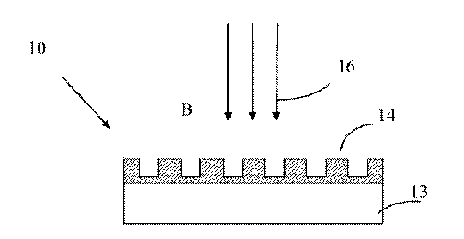
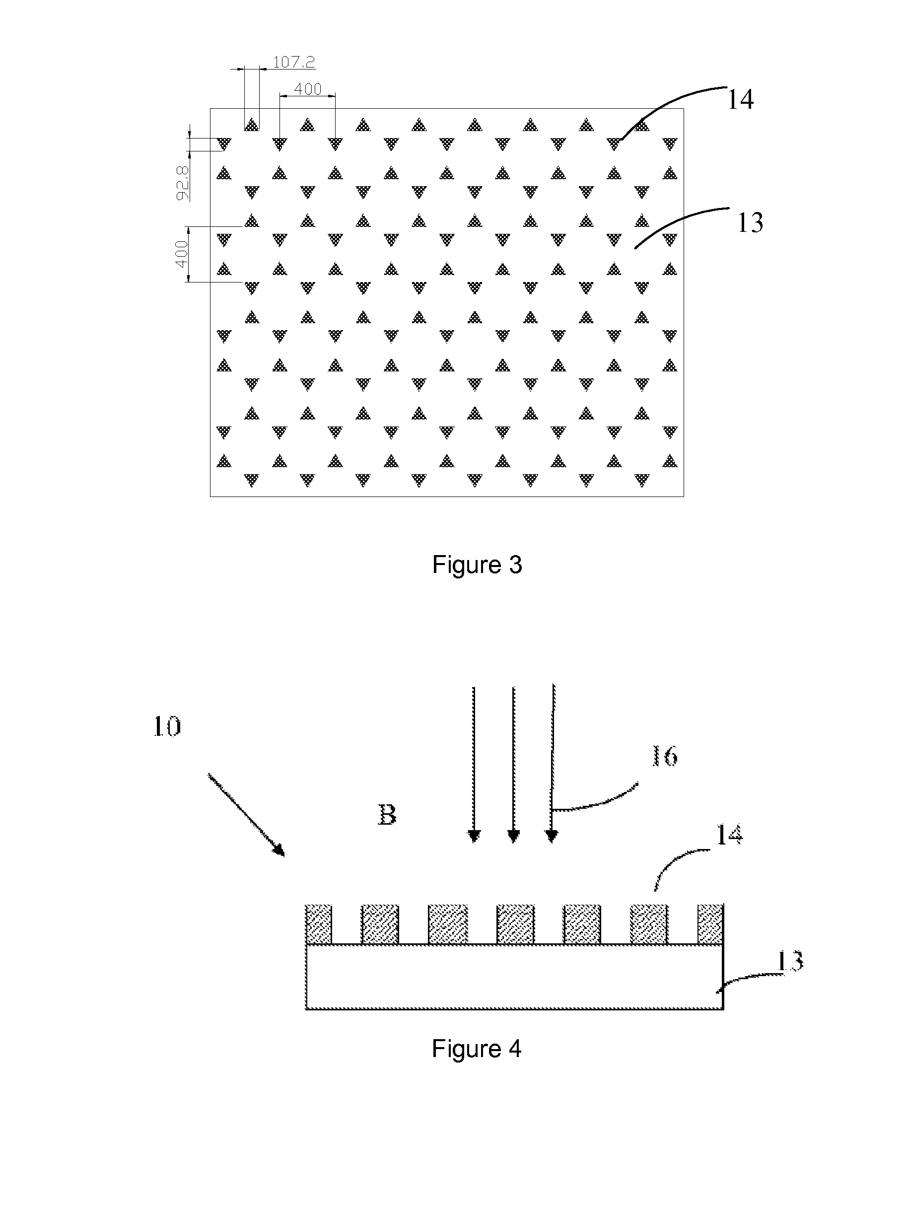
[0050]The basic structure of the glass light emitting element of the present Example having a metal film is shown in FIG. 1. A green luminescent glass 13 having a size of 1×1 cm2 and surface-polished with 30Na2O.6Y2O3.60SiO2.4Tb2O3 (the numbers before the oxides represent molar ratio) is selected, and a metal layer 14 having an orderly periodic structure formed by the combination of six triangular pyramid-shaped sliver particles is formed on its surface with the currently used micro-processing technique. The structure scheme thereof is shown in FIG. 3. The specific structural parameters are also shown in FIG. 3. The height of the silver nano-particles is 30 nm. The luminescent glass 13 and the metal layer 14 constitute the light emitting element of the present Example.

[0051]The light emitting element manufactured in the present Example is bombarded with cathode rays produced by an electron gun. The electron beam passes through the metal layer 14 and then excites the luminescent glas...

example 2

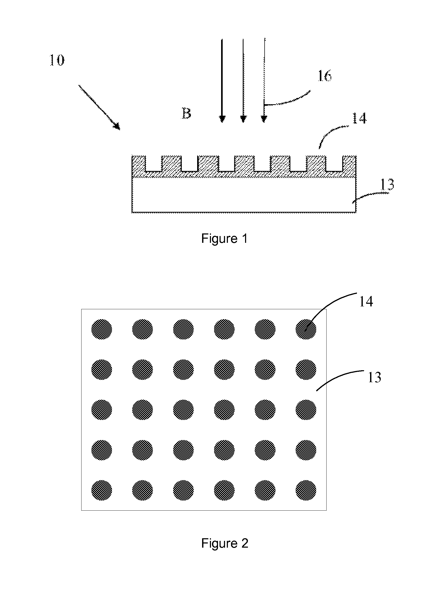
[0053]The basic structure of the glass light emitting element of the present Example having a metal film is shown in FIG. 1. A green luminescent glass 13 surface-polished with 30Na2O.6Y2O3.60SiO2.4Tb2O3 (the numbers before the oxides represent molar ratio) is used, and an array of cylindrical sliver nano-particles arranged in a square lattice as shown in FIG. 4 is formed on its surface with the currently used micro-processing technique. These constitute the light emitting element of the present Example.

[0054]The periodic metal micro and nano structure make it possible to control the surface plasmon by constructing the surface configuration of the metal structure and by regulating the size parameters, and the enhancement to the luminescence is wavelength-selective. Taking the metal nano-array of the present Example as an example, assuming that the peak radiation wavelength of the luminescent glass 13 is λ, the dielectric constant of the metal layer 14 is εm, and the dielectric consta...

example 3

[0055]The basic structure of the glass light emitting element of the present Example having a metal film is shown in FIG. 1. A red luminescent glass 13 as prepared by the above method and surface-polished with 30Na2O.6Y2O3.60SiO2.4Eu2O3 (the numbers before the oxides represent molar ratio) is used, and an aluminum layer having a periodic micro and nano structure as shown in FIG. 1 is formed on its surface with the currently used micro-processing technique. The period of the structure is 700 nm. The size of the metal particles is 200 nm. The height of the metal layer 14 is 50 nm. The depth of the concaves to the surface of the metal layer 14 is 10 nm. These constitute the light emitting element of the present Example.


PUM

PropertyMeasurementUnit
thicknessaaaaaaaaaa
thicknessaaaaaaaaaa
widthaaaaaaaaaa

Abstract

A light emitting element (10) is provided, which includes luminescent glass (13), a metal layer (14) formed on the surface of the luminescent glass (13), wherein periodic micro and nano structure is provided on the metal layer (14), and the chemical constituent of the luminescent glass (13) is rare-earth-ion doped silicate. Further provided are manufacturing and luminescence methods of the light emitting element. The luminescent glass (13) in the present invention includes a metal layer (14) with periodic micro and nano structure, which can enhance the luminous efficiency and luminous homogeneity and stability of the luminescent glass, and can be used on superluminescent and high-speed operating light emitting devices.

Description

TECHNICAL FIELD[0001]The present invention belongs to the technical field of luminescent materials, and specifically relates to a light emitting element having a glass substrate as a luminescent material, and methods for manufacturing and luminescence thereof.BACKGROUND ART[0002]Conventional materials used for luminescent matrix include fluorescent powders, nano-crystals, glasses, and the like. Comparing with crystals and fluorescent powders, glasses have transparency, hardness, as well as good chemical stability and optical properties. In addition, glasses may be readily processed into products with various sizes and shapes, such as display devices or illuminating sources with various sizes and shapes.[0003]For example, in the field of vacuum microelectronics, field emissive devices normally utilize a luminescent glass as the luminescent body, which shows broad application prospect in fields such as illumination and displays, and has drawn great attention from research entities fro...

Claims


Application Information

Patent Timeline
Patent Type & Authority Applications(United States)
IPC IPC(8): G01N21/64B05D5/06B32B3/30B32B15/04G02B1/10
CPCB82Y20/00Y10T428/24612C09K11/7792G02B5/0215G02B2207/101G02B5/008H01J29/20C03C4/12H01J63/04H01J63/06C03C3/095C03C17/06C03C2217/252C03C2217/254C03C2217/256C03C2217/262Y10T428/24545Y10T428/24331C09K11/7774C09K11/77742C09K11/77922
Inventor ZHOU, MINGJIEMA, WENBOLIU, YUGANG
Owner OCEANS KING LIGHTING SCI&TECH CO LTD
Why Eureka
Try Eureka