Magnetic nano-resonator

a nano-resonator and magnetic field technology, applied in the field of electromechanical nano-resonators, can solve the problems of system that is clearly not suitable for integration, and the structure is also not compatible with the manufacture of processing electronics of the typ

Active Publication Date: 2012-11-13
EDISON WELDING INSTITUTE INC +1
View PDF24 Cites 4 Cited by
  • Summary
  • Abstract
  • Description
  • Claims
  • Application Information

AI Technical Summary

Benefits of technology

[0010]At the same time, the beam serves as a support for a current loop which moves in a uniform magnetic field. A difference in potential appears at the terminals thereof and makes it possible to detect the movement of the beam. This current loop may be merged with the metal wire used for excitation.
[0011]This system makes it possible to obtain ground measurement results with extreme sensitivities. More generally, the electrical output signals have wide amplitudes and largely deviate from the background noise, which enables easy detection of the signal.
[0014]Therefore, the problem consists of finding a new electromagnetic resonator type device, of the nanometric type, which makes it possible to remedy the limitations of the devices currently known, and which is, in particular, suitable for integration, compatible preferentially with MOS type manufacture, and low in consumption.
[0015]More preferentially, such a device has low electrostatic coupling effects, and the lowest possible detection noise.
[0026]A device according to the invention is fully suitable for integration, with the processing electronics thereof while minimizing consumption. In particular, the electromagnetic means are substantially the same size as the associated mechanical element (i.e. the fixed element or the mobile element).
[0032]Means make it possible to circulate an alternating current in the current conductor, for example at least one frequency equal to, or close to, a resonance frequency of the mobile part.

Problems solved by technology

On the other hand, this system is clearly not suitable for integration and remains a laboratory measurement.
This structure is also not compatible with the manufacture of processing electronics of the type positioned close to a NEMS (of the co-integration or post-CMOS integration type).

Method used


Image

  • Magnetic nano-resonator
  • Magnetic nano-resonator
  • Magnetic nano-resonator

Examples


Embodiment Construction

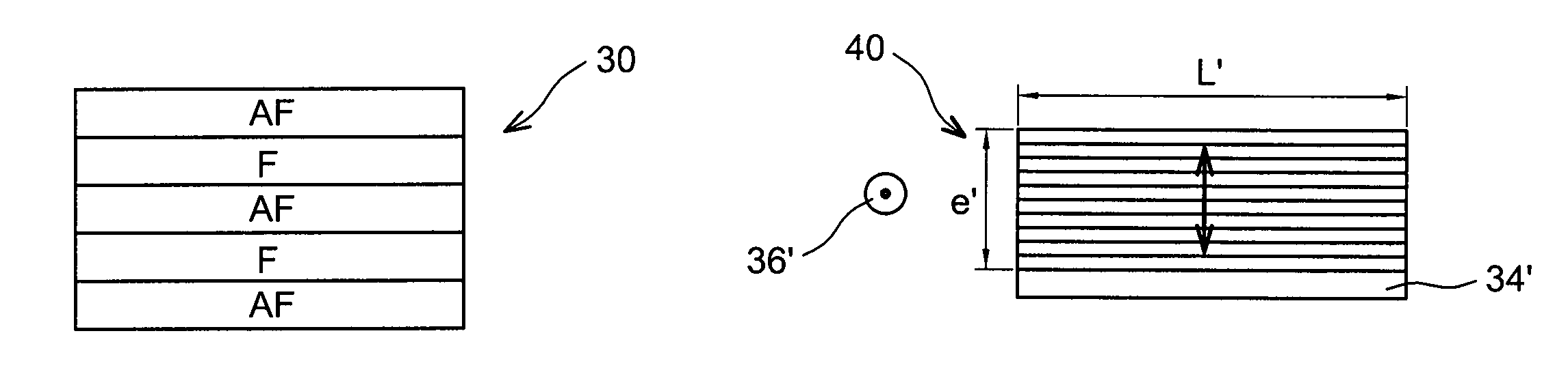
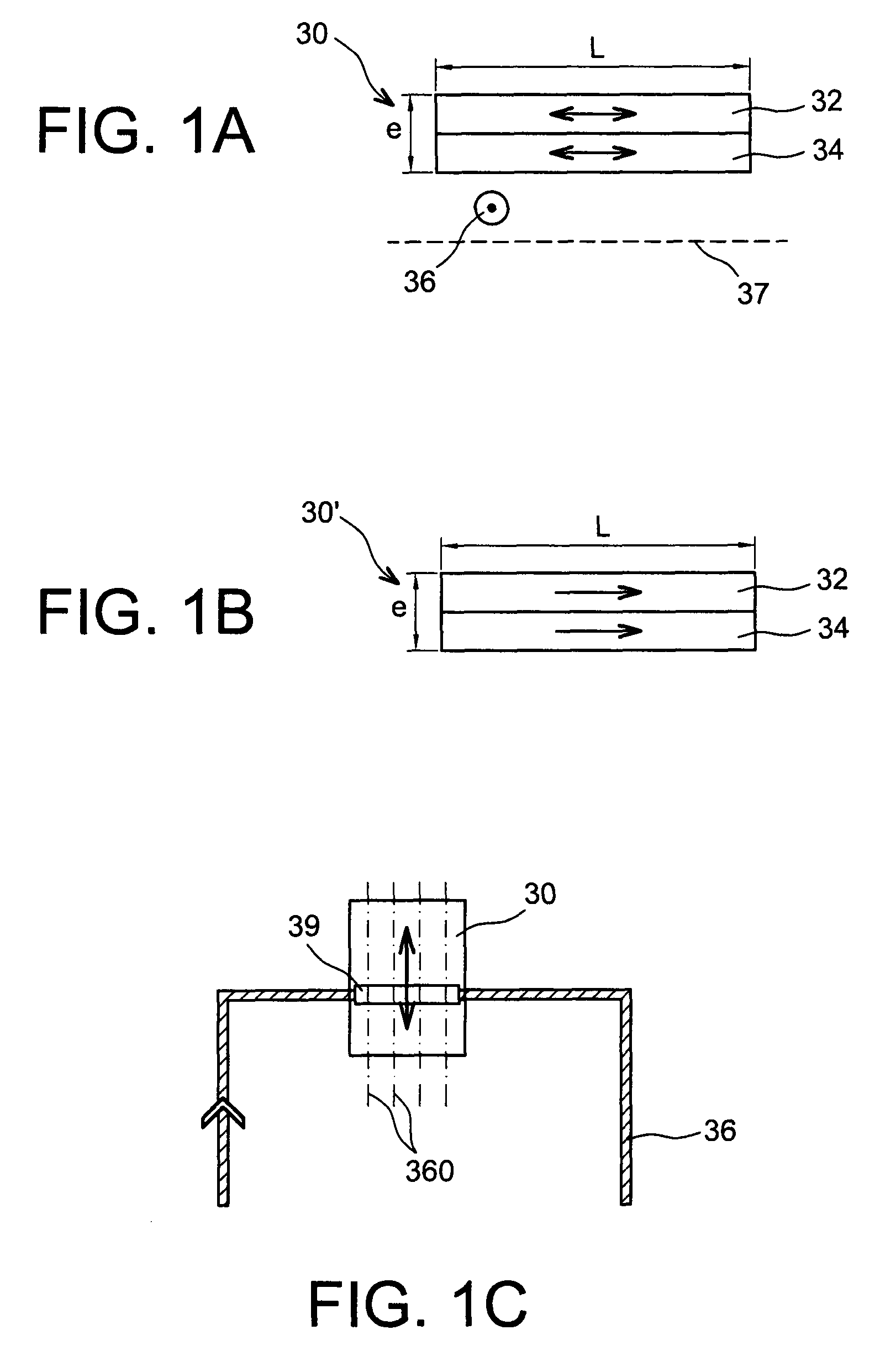
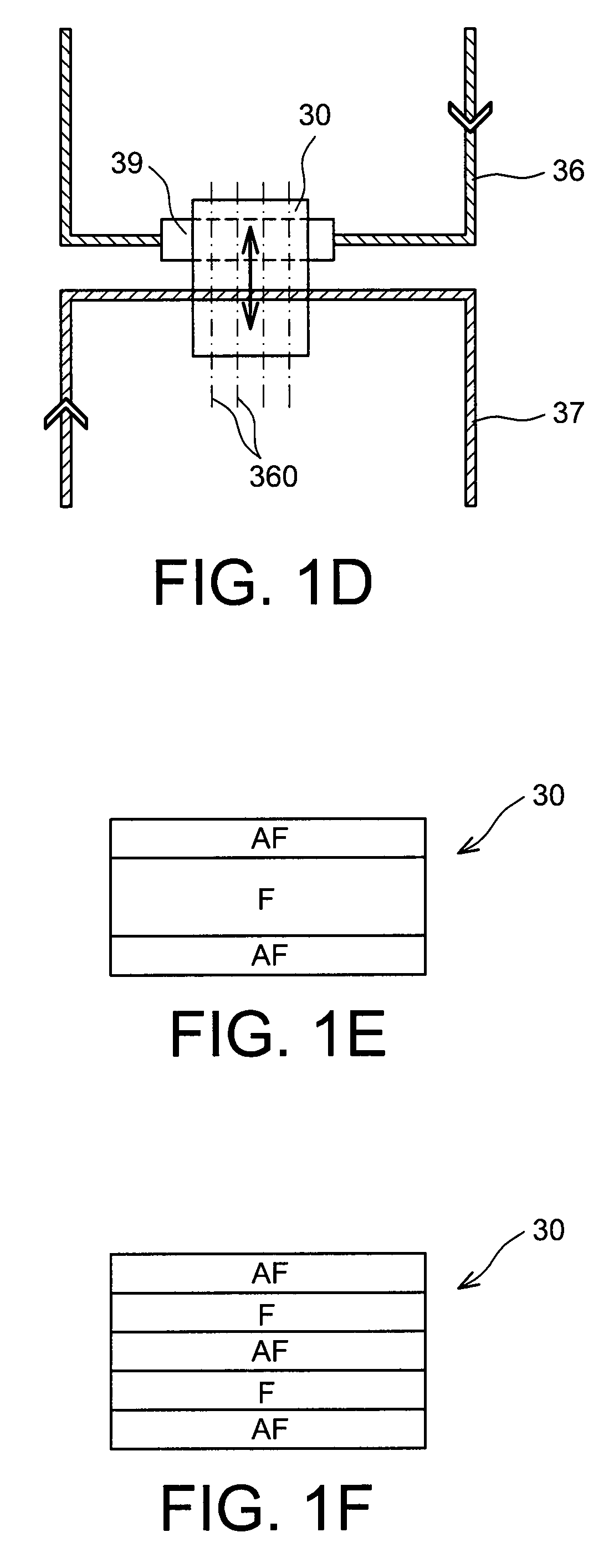
[0017]The invention relates to a resonator or nano-resonator device comprising:

[0018]at least one fixed element and at least one mobile element with respect to the fixed element,

[0019]first electromagnetic means, integrated or fixed on the fixed element, and second electromagnetic means, integrated or fixed on the mobile element, said electromagnetic means interacting to actuate the mobile element or to generate an oscillating movement of the mobile element.

[0020]The invention also relates to a resonator or nano-resonator device comprising:

[0021]at least one fixed element and at least one mobile element with respect to the fixed element,

[0022]first electromagnetic means, integrated or fixed on the fixed element, and second electromagnetic means, integrated or fixed on the mobile element, to generate, in interaction with the first electromagnetic means, an oscillating movement of the mobile element or to actuate the mobile element,

[0023]at least one of the first and second electromag...


PUM


Abstract

A nano-resonator device comprising at least one fixed element and at least one mobile element with respect to the fixed element, first electromagnetic means, integrated or fixed on the fixed element, and second electromagnetic means, integrated or fixed on the mobile element, to generate an oscillating movement of the mobile element.

Description

CROSS REFERENCE TO RELATED APPLICATIONS OR PRIORITY CLAIM[0001]This application claims priority to French Patent Application No. 08 52062, filed Mar. 28, 2008.DESCRIPTIONField of the Invention and State of the Related Art[0002]The invention relates to the field of electromechanical nano-resonators.[0003]Nano-resonators pave the way for multiple applications. They have applications in the field of “environmental” sensors, of the biological or chemical or temperature type. They may also find applications in inertial sensors (accelerometers, gyrometers).[0004]They may also be used in oscillators, as a time base or as filters.[0005]An electromechanical resonator is a mechanical structure vibrated by an external excitation means (electrodes in the case of electrical excitation) and wherein the deformation (or displacement) is detected by another means (other electrode or other transduction principle).[0006]The resonators may be classified according to the transduction and excitation mean...

Claims


Application Information

Patent Timeline
Patent Type & Authority Patents(United States)
IPC IPC(8): H03H9/24
CPCH03H3/0073H03H9/02259H03H9/2447H03H9/2457H03H9/2463G01R33/0286H03H2009/02511H03H2009/02519
Inventor DURAFFOURG, LAURENTANDREUCCI, PHILIPPEBILHAUT, LISEVIALA, BERNARD
Owner EDISON WELDING INSTITUTE INC
Why Eureka
Try Eureka