Substrate for semiconductor device including an island-shaped underlying film overlapping a transistor, method of manufacturing the same, semiconductor device and electronic device

a semiconductor device and substrate technology, applied in semiconductor/solid-state device manufacturing, semiconductor devices, semiconductor devices, etc., can solve the problems of substrate flexure, inaccurate size and position of substrate, etc., and achieve the effect of suppressing substrate flexur

Active Publication Date: 2012-12-11
E INK CORPORATION
View PDF9 Cites 13 Cited by
  • Summary
  • Abstract
  • Description
  • Claims
  • Application Information

AI Technical Summary

Benefits of technology

[0006]An advantage of some aspects of the invention is that it provides, for example, a substrate for a semiconductor device including a transistor on a substrate, which is capable of suppressing flexure in the substrate while meeting demands for resource saving and cost reduction, a method of manufacturing the same, a semiconductor device including such a substrate for the semiconductor device, and an electronic device including such a semiconductor device.

Problems solved by technology

However, there is a technical problem that is caused by the fact that when the underlying insulation film is formed over the entire surface of the substrate as disclosed in JP-A-2009-176828, flexure may occur in the substrate due to stress generated within the underlying insulation film in the formation steps thereof.
If the thickness of the underlying film is constant (that is, if the surface of the underlying film is flat), there may be a concern that the film after application is easily deviated on the underlying film, to thereby cause the size and position thereof to be inaccurate.

Method used


Image

  • Substrate for semiconductor device including an island-shaped underlying film overlapping a transistor, method of manufacturing the same, semiconductor device and electronic device
  • Substrate for semiconductor device including an island-shaped underlying film overlapping a transistor, method of manufacturing the same, semiconductor device and electronic device
  • Substrate for semiconductor device including an island-shaped underlying film overlapping a transistor, method of manufacturing the same, semiconductor device and electronic device

Examples


first embodiment

[0041]The electrophoretic display panel according to the first embodiment will be described with reference to FIGS. 1 to 5.

[0042]First, the whole configuration of the electrophoretic display panel according to the embodiment will be described with reference to FIGS. 1 and 2.

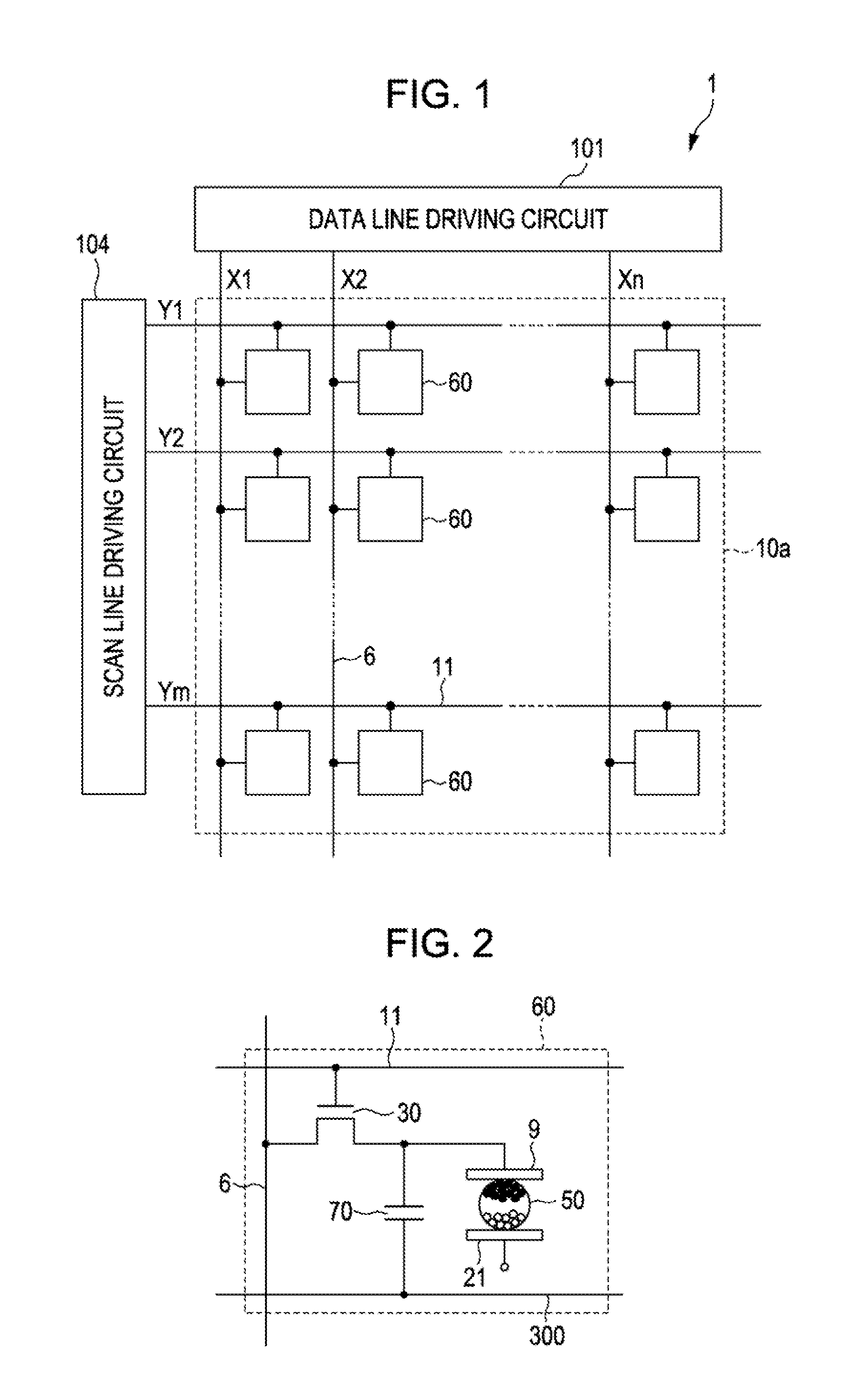
[0043]FIG. 1 is a block diagram illustrating the whole configuration of the electrophoretic display panel according to the embodiment.

[0044]In FIG. 1, an electrophoretic display panel 1 according to the embodiment has a display portion 10a in which pixels60 of m columns×n rows are arranged in a matrix shape (two-dimensionally). Here, m scan lines 11 (that is, scan lines Y1, Y2, . . . , Ym) and n data lines 6 (that is, data lines X1, X2, . . . , Xn) are provided to the display portion 10a so as to intersect each other. The m scan lines 11 extend in the row direction (that is, X direction), and n data lines 6 extend in the column direction (that is, Y direction). The pixels 60 are disposed so as to correspond to th...

second embodiment

[0084]Subsequently, the configuration of an electrophoretic display panel according to a second embodiment will be described with reference to FIG. 6. Meanwhile, the electrophoretic display panel according to the second embodiment has schematically the same structure as that of the electrophoretic display panel, described basically, according to the first embodiment. For this reason, description of the points in common with the first embodiment mentioned above will be not repeated, and description will be made focusing on the points different therefrom.

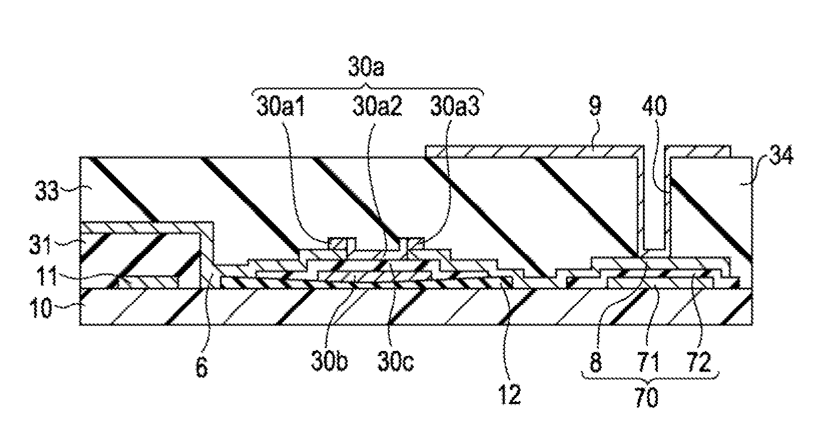
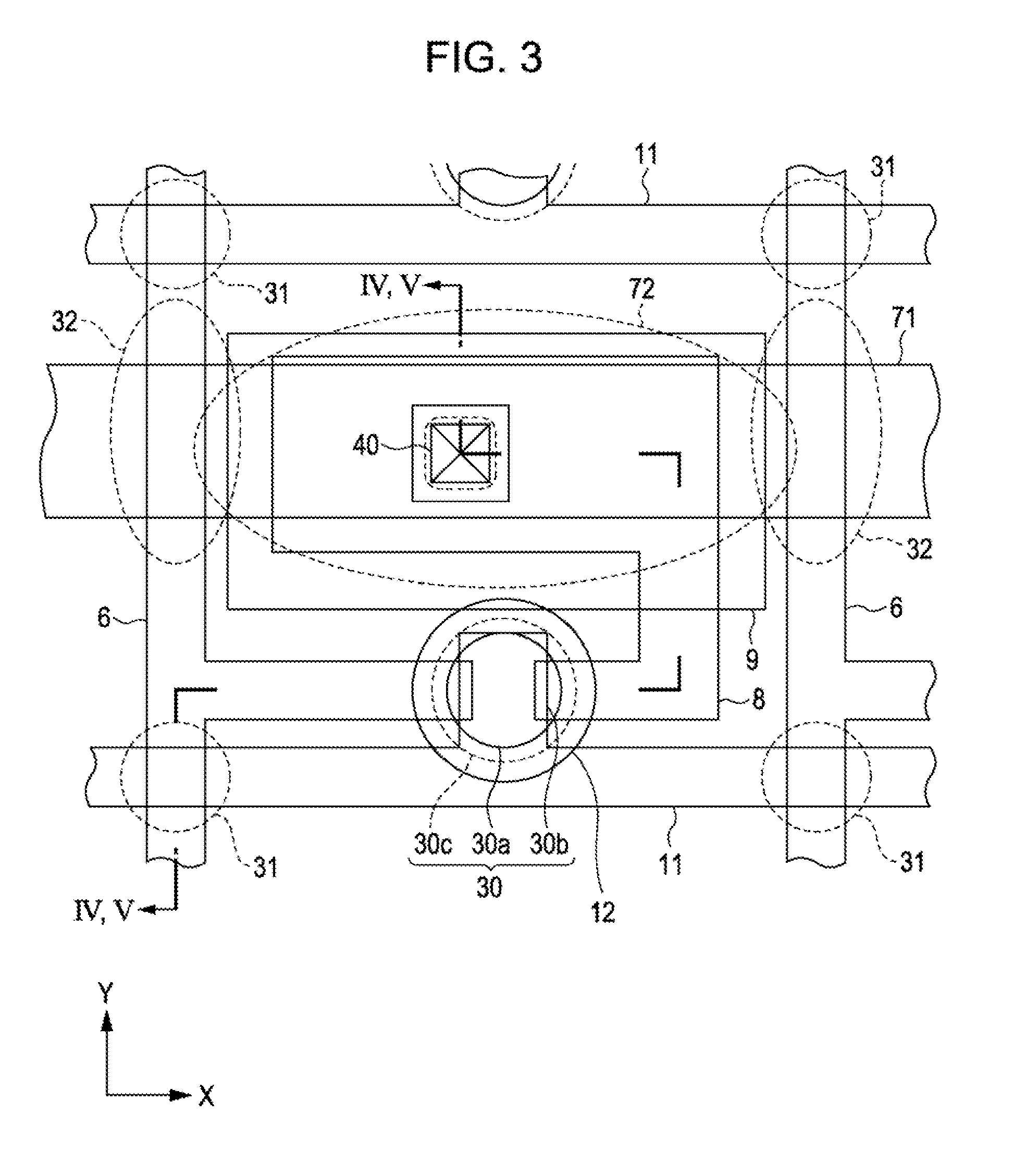
[0085]The TFT 30 according to the embodiment is a so-called bottom gate type transistor in which the gate electrode 30b, the gate insulating film 30c and the semiconductor layer 30a are laminated in order from the lower layer side.

[0086]The gate electrode 30b is directly formed on the surface of the underlying insulation film 12 formed on the surface of the element substrate 10. Here, the underlying insulation film 12 is formed in an ...


PUM


Abstract

A substrate for a semiconductor device is provided, including: a substrate; a transistor, formed on the substrate, that includes a semiconductor layer, and a gate electrode disposed so as to be opposed to the semiconductor layer with a gate insulating film interposed therebetween; and an underlying film disposed below the semiconductor layer, as an underlayer of the transistor, and formed in an island shape so as to at least partially overlap the semiconductor layer, in a plan view of the substrate.

Description

BACKGROUND[0001]1. Technical Field[0002]The present invention relates to a substrate for a semiconductor device, a method of manufacturing the same, a semiconductor device including the substrate for the semiconductor device, and an electronic device including the semiconductor device.[0003]2. Related Art[0004]An example of the substrate for the semiconductor device of this type includes an active matrix substrate, used in a display device such as, for example, an active matrix driving-type electrophoretic display device, which includes, on a substrate, a pixel electrode, and a thin film transistor (TFT) as a scan line, a data line and a pixel switching element for performing selective driving of this pixel electrode. In such an active matrix substrate, there may be a case where an underlying insulation film is provided on the substrate in order to planarize the irregularities existing on the surface of the substrate, and to effectively block degassing from the substrate, or gas, mo...

Claims


Application Information

Patent Timeline
Patent Type & Authority Patents(United States)
IPC IPC(8): H01L31/062
CPCH01L27/1248H01L27/1218H01L29/78603
Inventor SATO, TAKASHI
Owner E INK CORPORATION
Why Eureka
Try Eureka