Protective seal ring for preventing die-saw induced stress

a technology of sealing rings and die-sawing, which is applied in the direction of semiconductor devices, semiconductor/solid-state device details, electrical devices, etc., can solve the problems of not having enough strength to stop crack propagation, and achieve the effect of reducing the amount of crack propagation caused by die-sawing

Active Publication Date: 2012-12-18
TAIWAN SEMICON MFG CO LTD
View PDF109 Cites 29 Cited by
  • Summary
  • Abstract
  • Description
  • Claims
  • Application Information

AI Technical Summary

Benefits of technology

[0011]Advantageously, by using the embodiments of the presen...

Problems solved by technology

If this seal ring is damaged, there will be no structure for preventing cracks from propagating into the respective semiconductor chip.
Second, the continuous via bars oft...

Method used


Image

  • Protective seal ring for preventing die-saw induced stress
  • Protective seal ring for preventing die-saw induced stress
  • Protective seal ring for preventing die-saw induced stress

Examples


Embodiment Construction

[0018]The making and using of embodiments are discussed in detail below. It should be appreciated, however, that the embodiments provide many applicable inventive concepts that can be embodied in a wide variety of specific contexts. The specific embodiments discussed are merely illustrative of specific ways to make and use the invention and do not limit the scope of the invention.

[0019]Seal ring structures with improved crack prevention ability and methods of forming the same are provided. The variations of the embodiments are discussed. Throughout the various views and illustrative embodiments of the present invention, like reference numbers are used to designate like elements.

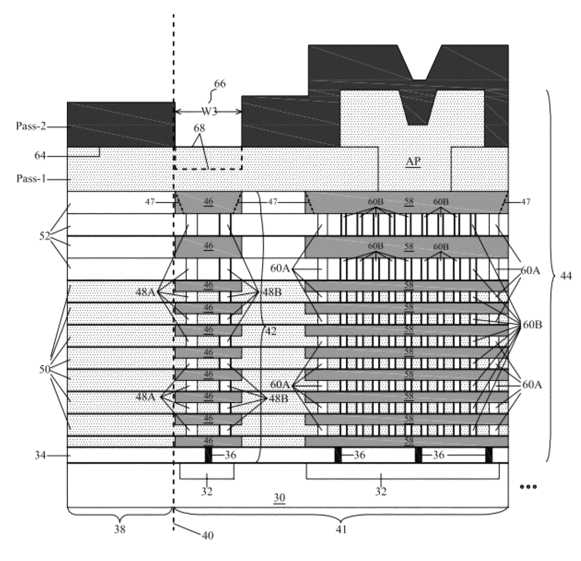
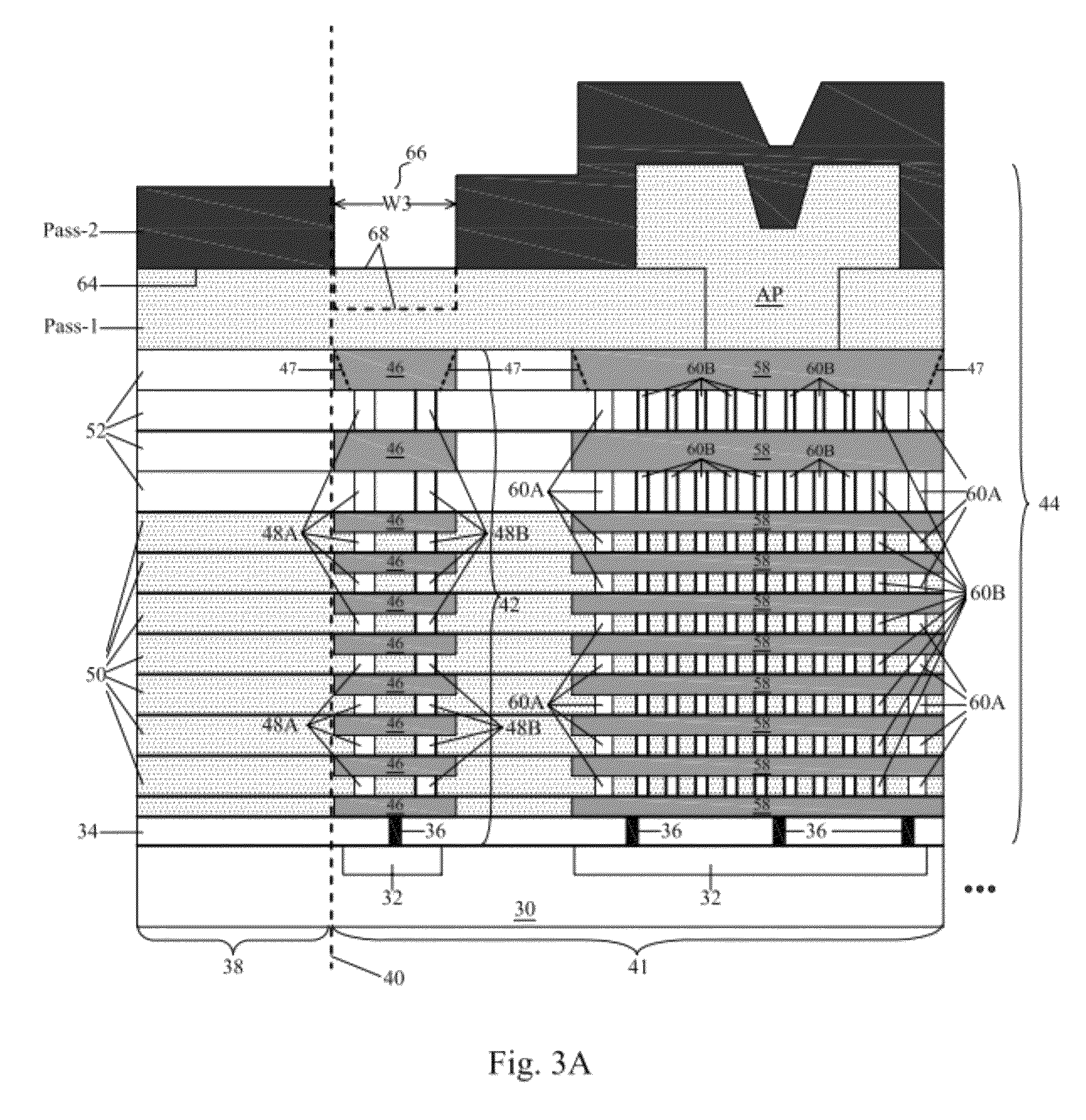
[0020]FIG. 3A illustrates a first embodiment of the present invention. A portion of a semiconductor wafer includes semiconductor substrate 30, which may be formed of silicon or other group III, group IV, and / or group V elements. Semiconductor substrate 30 may be lightly doped with a p-type impurity. Heavily d...


PUM


Abstract

A semiconductor chip includes a semiconductor substrate; a plurality of low-k dielectric layers over the semiconductor substrate; a first passivation layer over the plurality of low-k dielectric layers; and a second passivation layer over the first passivation layer. A first seal ring is adjacent to an edge of the semiconductor chip, wherein the first seal ring has an upper surface substantially level to a bottom surface of the first passivation layer. A second seal ring is adjacent to the first seal ring and on an inner side of the semiconductor chip than the first seal ring. The second seal ring includes a pad ring in the first passivation layer and the second passivation layer. A trench ring includes at least a portion directly over the first seal ring. The trench ring extends from a top surface of the second passivation layer down to at least an interface between the first passivation layer and the second passivation layer.

Description

[0001]This application claims the benefit of the following provisionally filed U.S. patent application: Application Ser. No. 61 / 076,046, filed Jun. 26, 2008, and entitled “Protective Seal Ring,” which application is hereby incorporated herein by reference.CROSS-REFERENCE TO RELATED APPLICATIONS[0002]This application relates to the following commonly-assigned U.S. patent applications: application Ser. No. 11 / 842,821, filed Aug. 21, 2007, and entitled “Seal Ring Structure with Improved Cracking Protection;” and application Ser. No. 11 / 933,931, filed Nov. 1, 2007, entitled “Seal Ring Structure with Improved Cracking Protection and Reduced Problems,” which applications are hereby incorporated herein by reference.TECHNICAL FIELD[0003]This invention relates to integrated circuits and more particularly to structures and formation methods of seal rings.BACKGROUND[0004]Seal ring formation is an important part in the back-end of semiconductor processes. Seal rings are stress protection struct...

Claims


Application Information

Patent Timeline
IPC IPC(8): H01L23/544
CPCH01L21/78H01L23/562H01L23/564H01L23/585H01L2924/0002H01L2924/00
Inventor JENG, SHIN-PUUCHEN, HSIEN-WEIHOU, SHANG-YUNTSAI, HAO-YIWU, ANBIARSHY N. F.LIU, YU-WEN
Owner TAIWAN SEMICON MFG CO LTD
Why Eureka
Try Eureka