Display device and electronic apparatus

a technology of electronic equipment and display device, which is applied in the direction of electrical equipment, semiconductor devices, instruments, etc., can solve the problems of affecting the reference electric potential

Inactive Publication Date: 2013-01-01
SONY CORP
View PDF9 Cites 6 Cited by
  • Summary
  • Abstract
  • Description
  • Claims
  • Application Information

AI Technical Summary

Benefits of technology

[0010]Therefore, there is a need for providing technology for preventing luminance changes due to formation of parasitic capacitance between an electrode of an auxiliary capacitor of one pixel of adjacent pixels and an electrode of the other pixel.
[0015]According to the embodiments of the present invention, in a circuit configuring a pixel, luminance changes due to formation of parasitic capacitance between an electrode of an auxiliary capacitor of one pixel of adjacent pixels and an electrode of the other pixel can be prevented.

Problems solved by technology

As a result, there is a problem in that the reference electric potential is affected by the parasitic capacitance so as to decrease the luminance.

Method used


Image

  • Display device and electronic apparatus
  • Display device and electronic apparatus
  • Display device and electronic apparatus

Examples


first example

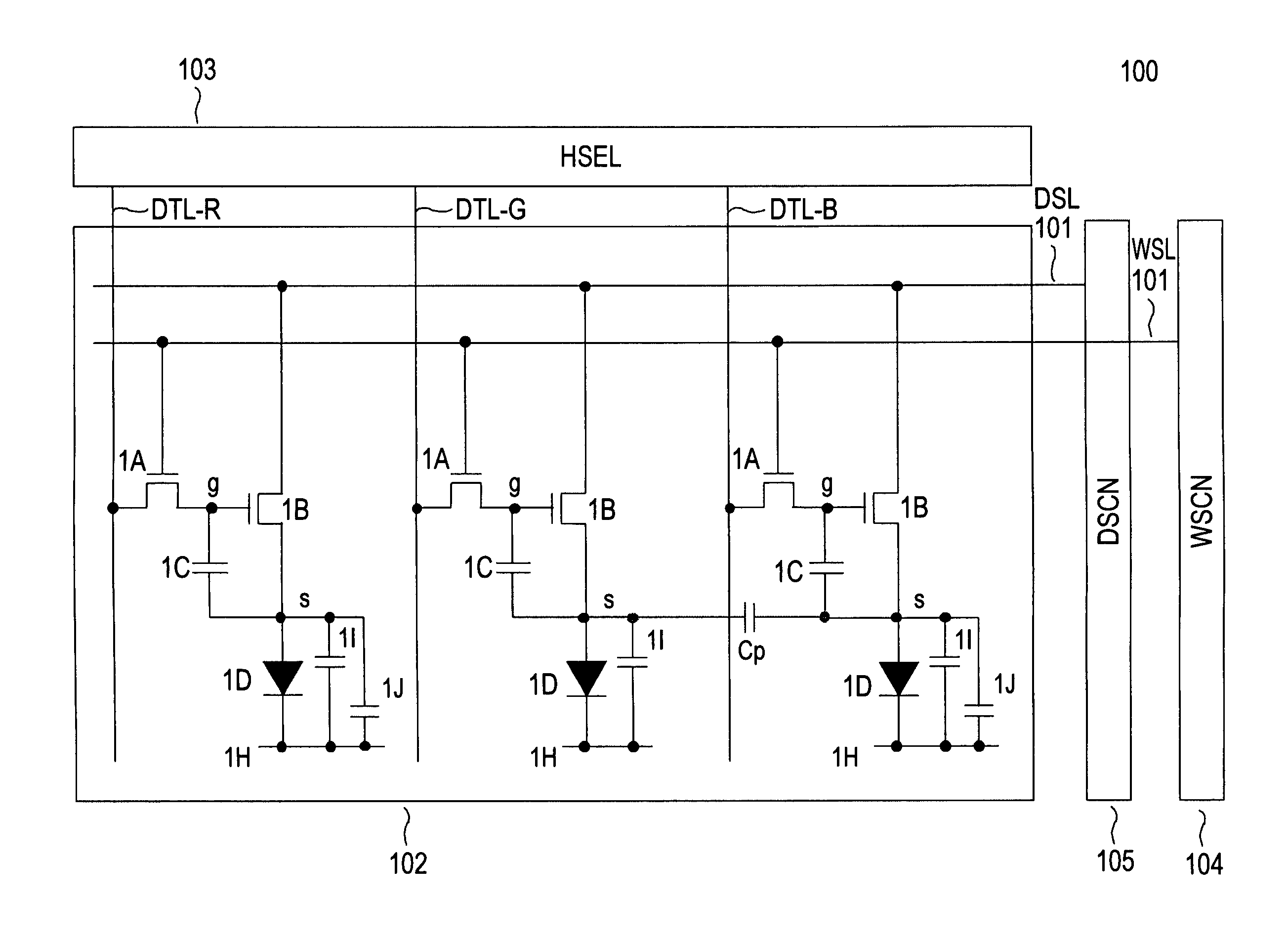
[0120]FIG. 15 is a schematic plan view illustrating an example (first example) of a pixel structure according to this embodiment. FIG. 15 represents the disposition configuration of an R (red) pixel, a G (green) pixel, and a B (blue) pixel. Each pixel is configured between the power supply line DSL and the scanning line WSL that extend in the horizontal direction (horizontal direction in the figure), and areas of the RGB pixels are partitioned by signal lines DTL that extend in the vertical direction (the vertical direction in the figure).

[0121]Within the area of each pixel, a writing transistor 1A, a driving transistor 1B, and a holding capacitor 1C are disposed. In addition, an auxiliary capacitor 1J that is used for adjusting a writing gain or a mobility correcting time is also disposed.

[0122]In the example represented in FIG. 15, a case is shown where the pattern density of the G (green) pixel is lower than that of the R (red) pixel, and the pattern density of the B (blue) pixel...

second example

[0133]FIG. 18 is a schematic cross-sectional view illustrating an example (second example) of a pixel structure according to this embodiment. This schematic cross-sectional view is a cross-sectional view taken along line A-A shown in FIG. 15. In this pixel structure, the auxiliary capacitor 1J of the B (blue) pixel is set in the area of the B (blue) pixel to the G (green) pixel. In addition, a shield electrode SD is disposed between the auxiliary capacitor 1J and the anode electrode AD-G of the G (green) pixel.

[0134]The lower electrode D1 of the auxiliary capacitor 1J of the B (blue) pixel is configured by the first metal wiring and is set as the cathode 1H of the organic EL element. On the other hand, the upper electrode D2 of the auxiliary capacitor 1J of the B (blue) pixel is configured by polysilicon as a middle layer and is set as the source s of the driving transistor, that is, the anode of the organic EL element.

[0135]Under such a configuration, according to this embodiment, ...


PUM


Abstract

A display device includes: a pixel array unit having pixels including a circuit configuration, in which a first electrode of an electro-optical element and a source electrode of a driving transistor are connected together, a gate electrode of the driving transistor and a source electrode or a drain electrode of a writing transistor are connected together, a holding capacitor is connected between the gate electrode and the source electrode of the driving transistor, and an auxiliary capacitor is connected between the first electrode and a second electrode of the electro-optical element, disposed on a substrate in a matrix shape, wherein, from one pixel of adjacent pixels to an area of the other pixel, the auxiliary capacitor of the one pixel is set to be disposed, and an electrode of the auxiliary capacitor that is disposed on the electro-optical element side is conductive with the second electrode of the electro-optical element.

Description

BACKGROUND OF THE INVENTION[0001]1. Field of the Invention[0002]The present invention relates to a display device and an electronic apparatus, and more particularly, to a flat type (flat panel type) display device formed by disposing pixels including electro-optical elements in a matrix form and an electronic apparatus using the display device.[0003]2. Description of the Related Art[0004]Recently, in the field of display devices that perform image display, flat type display devices formed by disposing pixels (pixel circuits) including light emitting elements in a matrix form have been spreading rapidly. As the flat type display devices, organic EL display devices using organic EL (electroluminescence) elements that utilize a phenomenon of light emission at the time of applying an electric field, for example, to an organic thin film have been developed and commercialized.[0005]The organic EL display device has the following features. The organic EL element can be driven by an applica...

Claims


Application Information

Patent Timeline
Patent Type & Authority Patents(United States)
IPC IPC(8): H01L27/14
CPCG09G3/3233H01L27/1255H01L27/3265G09G5/003G09G5/026H01L33/005H01L33/08H01L27/12G09G2300/0819G09G2300/0842G09G2300/0852G09G2300/0866G09G2320/0219G09G2320/043H01L27/3211H01L27/13G09G2300/0452H10K59/35H10K59/1216H10K50/81H10K59/131H10K59/1213G09G3/3258G09G3/3266G09G2300/0426G09G2320/0233
Inventor ASANO, MITSURUIIDA, YUKIHITO
Owner SONY CORP
Why Eureka
Try Eureka