
LED package and back light unit using the same

a technology of led packages and backlight units, applied in the field of side view led packages having an elongated cavity, can solve the problems of inefficiency of conventional side view led packages, difficult control of light properties, and other types of led packages, etc., and achieve the effect of suppressing enlargement, and not substantially increasing the distance of light emitting paths

Inactive Publication Date: 2013-01-29
SEOUL SEMICONDUCTOR
View PDF18 Cites 17 Cited by
  • Summary
  • Abstract
  • Description
  • Claims
  • Application Information

AI Technical Summary

Benefits of technology

This design allows for precise control of light orientation angles, enhances light efficiency, and minimizes the increase in package thickness and size, enabling a compact and efficient LED package suitable for backlight units.

Problems solved by technology

However, in the conventional side view LED package, it is limited to adjust an orientation angle of light emitted from the LED chip 17, and it is difficult to control the properties of light, including an orientation angle and the like, only by the limited shape of the cavity and encapsulant filled therein.
Further, the conventional side view LED package is inefficient because a large number of LED packages are required to supply light parallel with a light guide plate.
In addition to the side view LED package, another type of LED package, e.g., a top view LED package, also has a limit in adjusting an orientation angle of light emitted from an LED chip.
However, a conventional side view LED package does not provide a uniform light in a backlight unit since it is difficult to control an orientation angle.
However, such a technique is easily applied to a top view LED package having a circular cavity, but it is difficult to apply the technique to an LED package having a small thickness and an elongated and narrow cavity, such as a side view LED package.
In addition, when a lens is mounted on an upper surface of a body of an LED package, the entire size of an optical system is increased and light loss results from the increase of the distance of a path through which light emits to the outside via an encapsulant and the lens.

Method used


Image

  • LED package and back light unit using the same
  • LED package and back light unit using the same
  • LED package and back light unit using the same

Examples


Embodiment Construction

[0037]Hereinafter, preferred embodiments of the present invention will be described in detail with reference to the accompanying drawings. The following embodiments are provided only for illustrative purposes so that those skilled in the art can fully understand the spirit of the present invention. Therefore, the present invention is not limited to the following embodiments but may be implemented in other forms. In the drawings, the widths, lengths, thicknesses and the like of elements may be exaggerated for convenience of illustration. Like reference numerals indicate like elements throughout the specification and drawings.

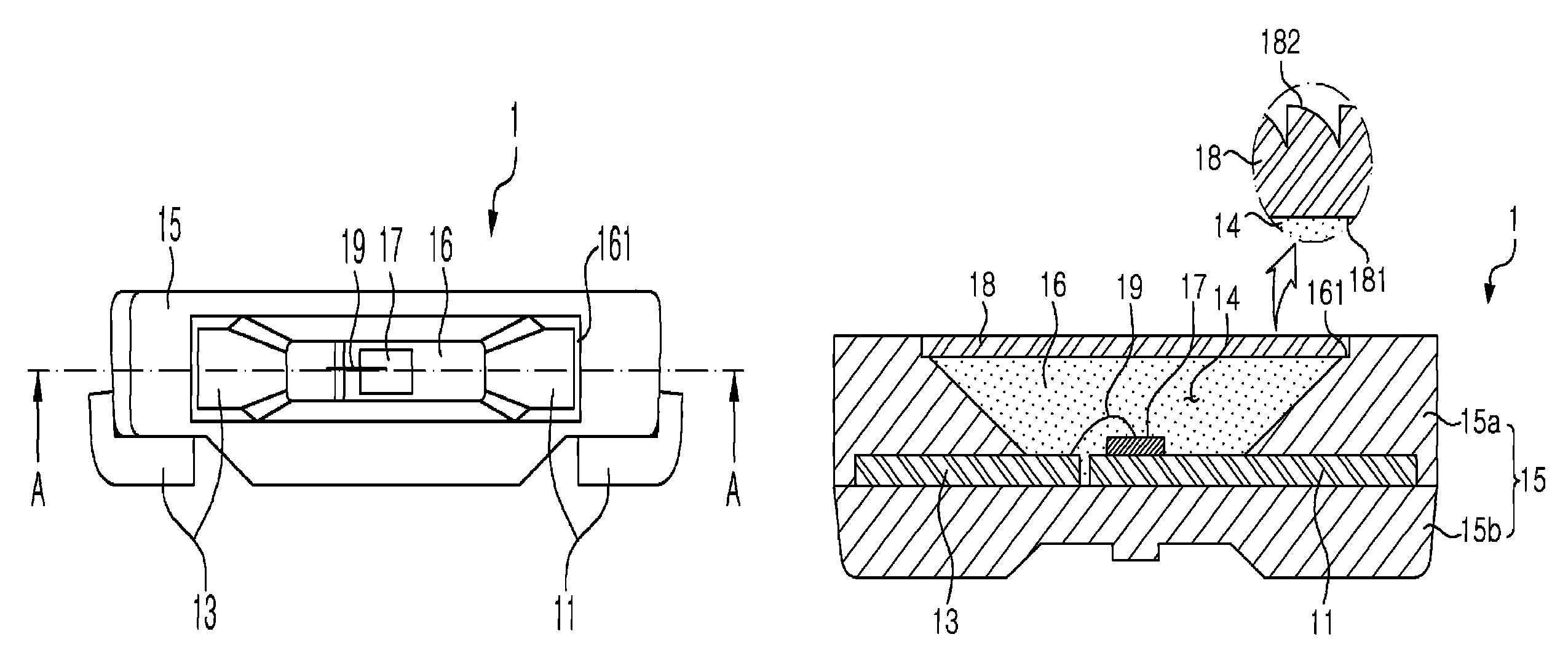
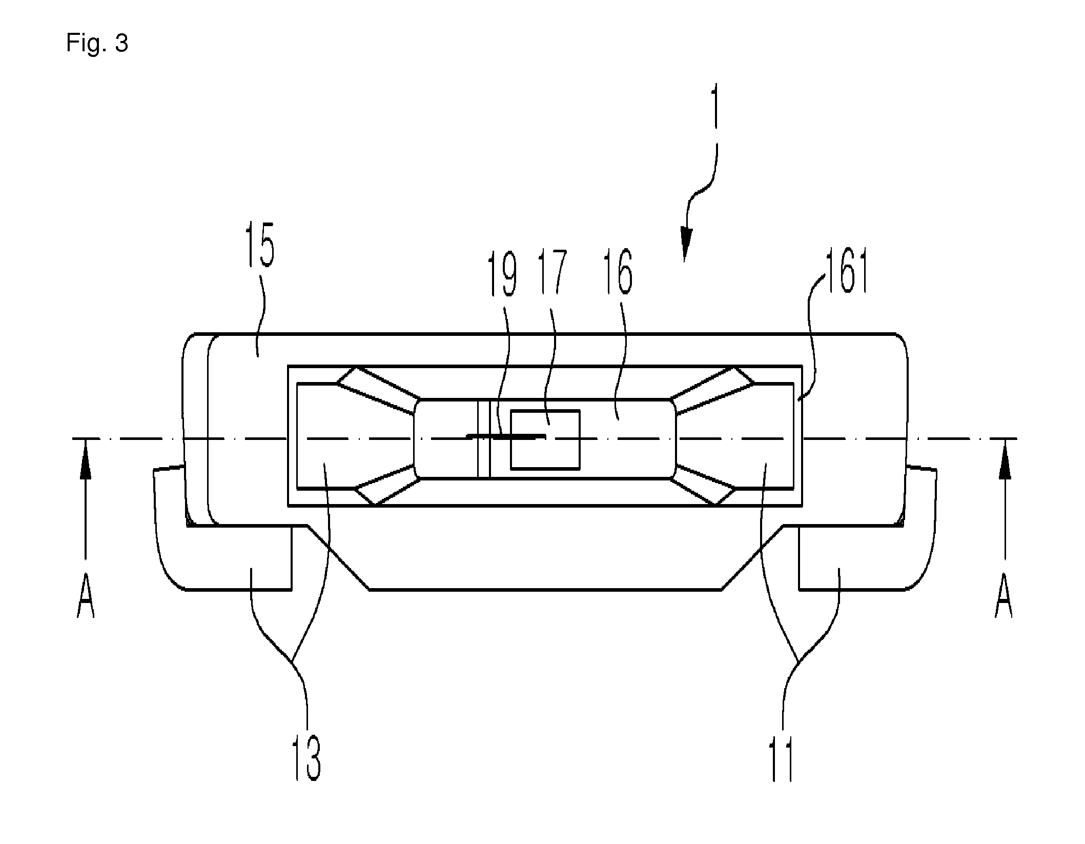
[0038]FIG. 3 is a plan view illustrating a side view LED package according to an embodiment of the present invention, and FIG. 4 is a sectional view taken along line A-A of FIG. 3. In FIG. 3, an encapsulant and a lens, which are formed in the inside of a cavity, are omitted such that the inside of the cavity can be seen. In FIG. 4, the encapsulant and the lens ca...


PUM


Abstract

Disclosed is a light emitting diode (LED) package. The LED package comprises a package body having a cavity and a stepped portion positioned on a top portion of the cavity; an LED chip mounted on a bottom surface of the cavity; an encapsulant formed in the cavity to cover the LED chip; and a lens having a pattern and attached to the stepped portion on the encapsulant.

Description

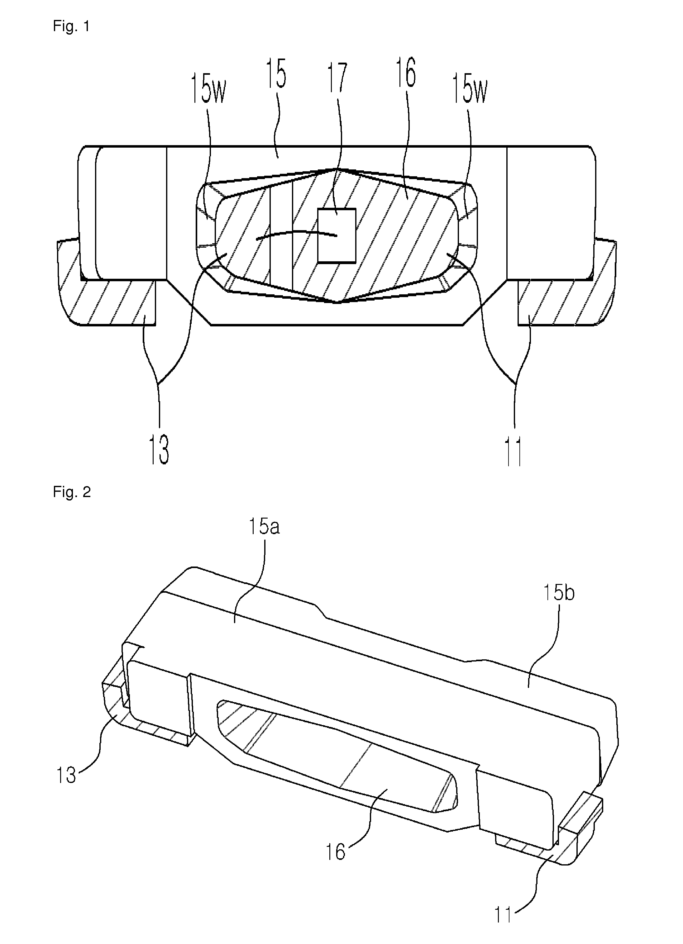
CROSS-REFERENCE TO RELATED APPLICATIONS[0001]This application is the National Stage of International Application No. PCT / KR2008 / 005544, filed Sep. 19, 2008, and claims priority from and the benefit of Korean Patent Application No. 10-2007-0098343, filed on Sep. 28, 2007, and Korean Patent Application No. 10-2007-0141377, filed on Dec. 31, 2007, which are all hereby incorporated by reference for all purposes as if fully set forth herein.BACKGROUND OF THE INVENTION[0002]1. Field of the Invention[0003]The present invention relates to a light emitting diode (LED) package, and more particularly, to a side view LED package having an elongated cavity.[0004]2. Discussion of the Background[0005]LED packages are formed by mounting an LED chip to various types of packages depending on use. Particularly, a side view LED package is mainly used as a display backlight source, and is disposed at a side of a light guide plate to provide light in parallel with the light guide plate.[0006]FIGS. 1 and ...

Claims


Application Information

Patent Timeline
Patent Type & Authority Patents(United States)
IPC IPC(8): H01L33/00H01L33/58
CPCH01L33/58H01L2224/48091H01L2224/48247H01L2924/00014
Inventor KIM, TAE KWANGLEE, CHUNG HOONKIM, DO HYUNGRYU, SEUNG RYEOLJEONG, CHAN SUNGHWANG, WOONG JOON
Owner SEOUL SEMICONDUCTOR
Learn More