
Touch pad and electronic device having the same

a technology of electronic devices and touch pads, which is applied in the direction of mechanical pattern conversion, pulse technique, instruments, etc., can solve the problems of increased manufacturing costs, complicated structure, and difficulty in manufacturing touch pads with slim designs, and achieve the effect of reducing manufacturing costs and simplifying structur

Active Publication Date: 2013-02-19
HEWLETT PACKARD DEV CO LP
View PDF17 Cites 30 Cited by
  • Summary
  • Abstract
  • Description
  • Claims
  • Application Information

AI Technical Summary

Benefits of technology

[0009]The present general inventive concept provides a touch pad with a simplified structure and reduced manufacturing costs by mounting components on a single board and forming an LED integrally with a cover frame.
[0010]The present general inventive concept also provides an electronic device which is made slimmer and has an improved external design by including the above-described touch pad.
[0016]The touch pad may further include a double-sided adhesive tape to form a secure connection between the cover frame and the board and to prevent air from entering between the cover frame and the board.
[0024]The cover frame may be securely fastened to the circuit board to prevent air bubbles from forming between the cover frame and the circuit board.

Problems solved by technology

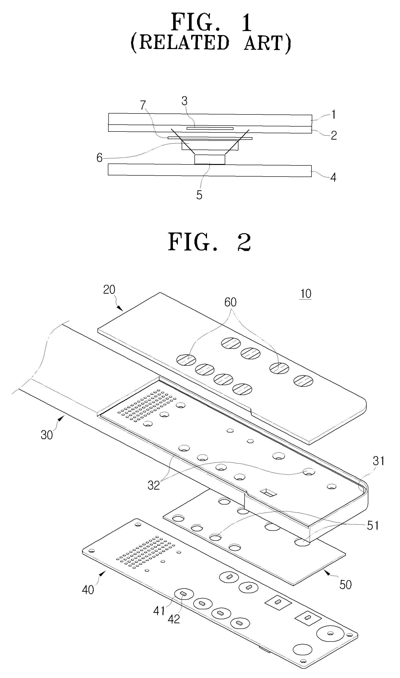
However, the conventional touch pad as constructed above requires the first board 2 including the touch sensor 3 mounted thereon, and the second board 4 including the LED 5 mounted thereon, so the structure is complicated.
Additionally, since the LED holder 6 and diffusion sheet 7, which are required to diffuse light, are placed between the first and second boards 2 and 4, it is difficult to manufacture the touch pad with a slim design, and manufacturing costs may increase.

Method used


Image

  • Touch pad and electronic device having the same
  • Touch pad and electronic device having the same
  • Touch pad and electronic device having the same

Examples


Embodiment Construction

[0036]Reference will now be made in detail to the embodiments of the present general inventive concept, examples of which are illustrated in the accompanying drawings, wherein like reference numerals refer to the like elements throughout. The embodiments are described below in order to explain the present general inventive concept by referring to the figures.

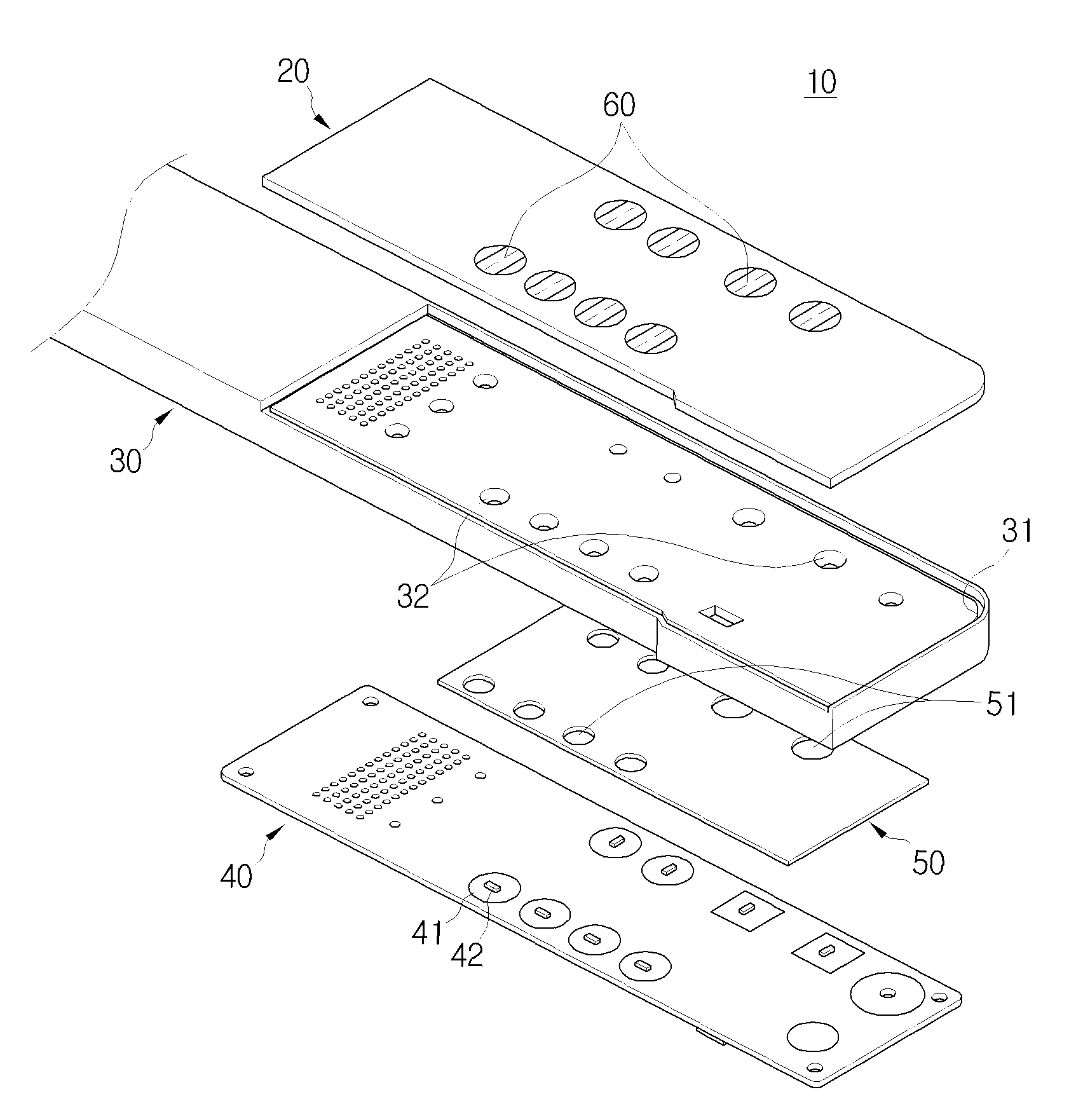
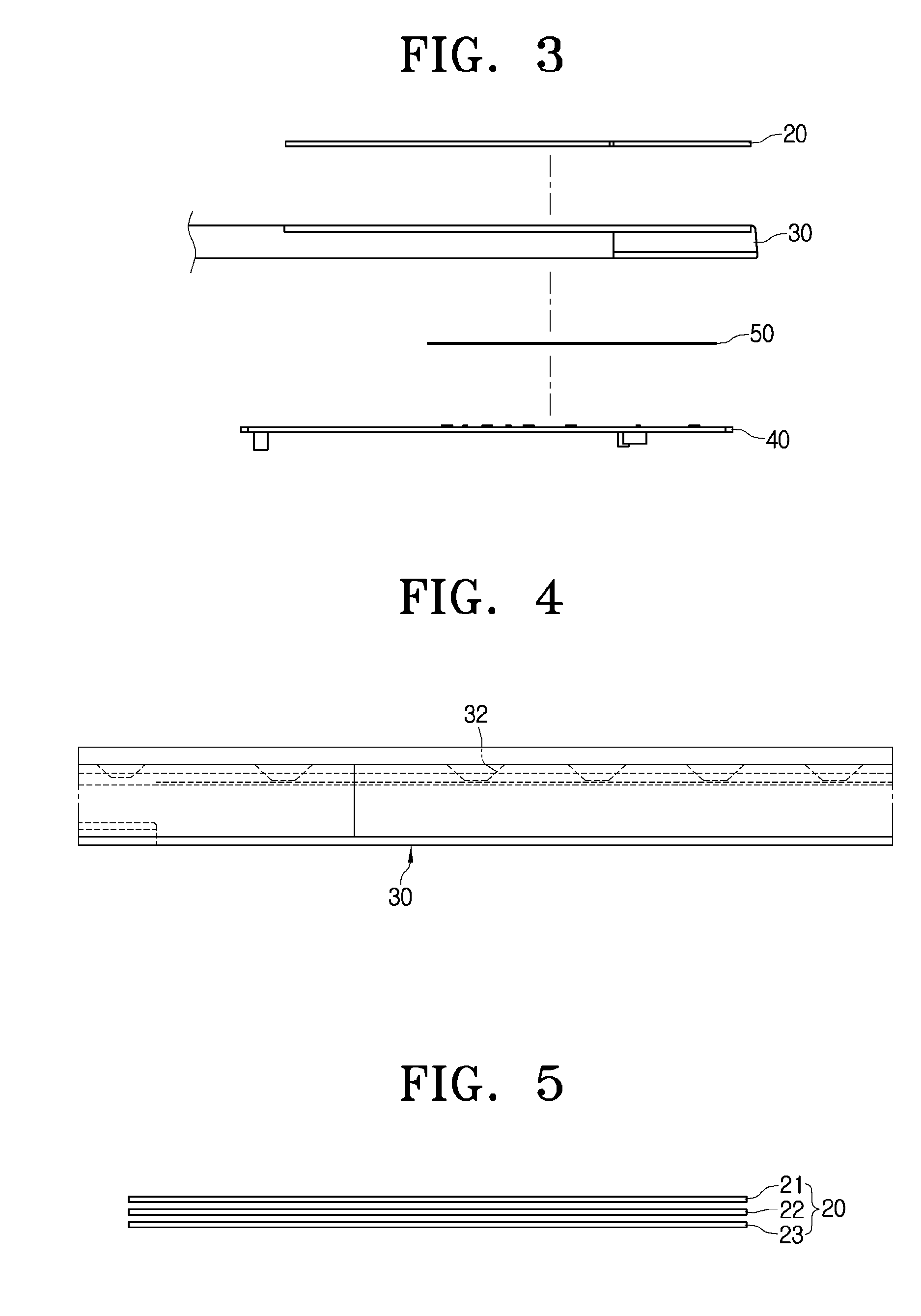
[0037]As illustrated in FIGS. 2 through 5, a touch pad 10 according to an exemplary embodiment of the present general inventive concept includes a cover 20, a cover frame 30, a board 40, and a double-sided adhesive tape 50.

[0038]The cover 20 may be formed of a transparent polycarbonate sheet or an acryl sheet, though it is not limited to such materials, and the cover 20 may be formed using a transparent polycarbonate sheet. Referring to FIG. 5, the cover 20 includes a transparent polycarbonate sheet 21, a function icon film 22 which is printed on a rear surface of the polycarbonate sheet 21 and includes a plurality of function i...


PUM


Abstract

A touch pad with a simple structure to enable an electronic device to be manufactured more slimly and with low manufacturing costs. The touch pad includes a cover having a plurality of function icons a cover frame to support the cover, the cover frame including a plurality of light guide hollows, and a board, which is engaged with the cover frame and includes touch sensors and luminous elements to illuminate the function icons mounted thereon, the touch sensors and luminous elements being respectively mounted at positions on the board corresponding to the plurality of function icons.

Description

CROSS-REFERENCE TO RELATED APPLICATIONS[0001]This application claims priority under 35 U.S.C. §119 (a) of Korean Patent Application No. 10-2007-0027708, filed on Mar. 21, 2007, in the Korean Intellectual Property Office, the disclosure of which is incorporated herein by reference in its entirety.BACKGROUND OF THE INVENTION[0002]1. Field of the Invention[0003]The present general inventive concept relates to an input device of an electronic device, such as a printer, a copier, a multi-function machine, a portable terminal, etc. More particularly, the present general inventive concept relates to a touch pad and an electronic device having the touch pad.[0004]2. Description of the Related Art[0005]Input devices of electronic devices, such as printers, copiers, multi-function machines, portable terminals, etc., have rapidly changed from being button-based to being touch-based. Touch pads, as an example of touch-based input devices of electronic devices, allow products to be manufactured ...

Claims


Application Information

Patent Timeline
Patent Type & Authority Patents(United States)
IPC IPC(8): G06F3/041
CPCG06F3/0202G06F3/023H04N1/00392G06F3/041H04N1/04H03K2217/960785
Inventor YOON, WOON-SANGKIM, DO-KYUM
Owner HEWLETT PACKARD DEV CO LP
Learn More