FinFET with separate gates and method for fabricating a finFET with separate gates

a technology of finfet and separate gates, which is applied in the direction of basic electric elements, electrical apparatus, semiconductor devices, etc., can solve the problems of complex processing, high cost, and inability to meet the requirements of processing, and achieve the effect of reducing the cost of processing

Active Publication Date: 2013-03-05
UNITED MICROELECTRONICS CORP
View PDF13 Cites 5 Cited by
  • Summary
  • Abstract
  • Description
  • Claims
  • Application Information

AI Technical Summary

Benefits of technology

[0023]The method of the present invention also has the advantage of being sufficiently insensitive to process variations and misalignments. It exhibits a sufficient tolerance regarding the lateral positioning of the contact opening with respect to the fin and regarding the precision of the positioning of the end face of the remaining parts of the first gate layer in the removal step. The method of the first aspect of the invention thus provides a surprisingly simple technology to manufacture FinFETs with separate gates.
[0044]The FinFET has a structure that on one hand reflects and on the other hand enables the processing according to the method of the first aspect of the invention. The structure allows the use of a fabrication technology that forms the gate separation layer together with a second (replacement) gate-isolation layer only after the basic FinFET structure has been fabricated, by way of deposition of the mentioned second gate-isolation layer. It thus allows achieving the advantages of the methods of the first and second aspects of the invention and their embodiments.

Problems solved by technology

Considering the small dimensions of the fin in current and future MOS technology nodes, this processing is not only very tedious but also very sensitive to process variations and misalignment.
Furthermore, the integration of the FinFET processing of U.S. Pat. No. 6,611,029 B1 into conventional MOS processing schemes is very expensive.
In addition, the fabrication of a combination of a first type of FinFETs having two separated gates with a second type of FinFETs having a single continuous gate on a single wafer would be very costly on the basis of the method known from U.S. Pat. No. 6,611,029 B1.
The CMP treatment that separates the gates into two gate layers affects the whole wafer and does not allow differentiating between the FinFETs of the first and second type.
As a consequence, the FinFETs of the second type would either have to be fabricated separately after the FinFETs of the first type, or some kind of repair of the gate layer would have to be selectively performed on the FinFETs of the second type, which would require special efforts to avoid extensive defect formation in the gate stack and thus poor device performance.
Furthermore, the mentioned prior art does not address a situation, in which different gate-electrode materials are needed, e.g. for NMOS and PMOS transistors.

Method used


Image

  • FinFET with separate gates and method for fabricating a finFET with separate gates
  • FinFET with separate gates and method for fabricating a finFET with separate gates
  • FinFET with separate gates and method for fabricating a finFET with separate gates

Examples


Embodiment Construction

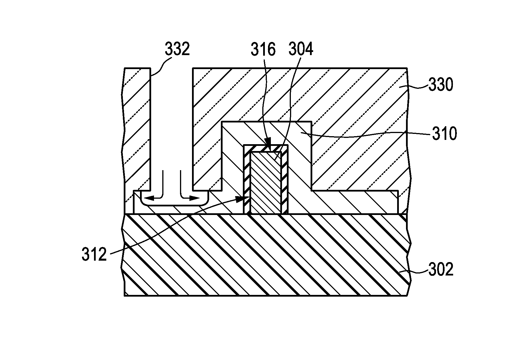
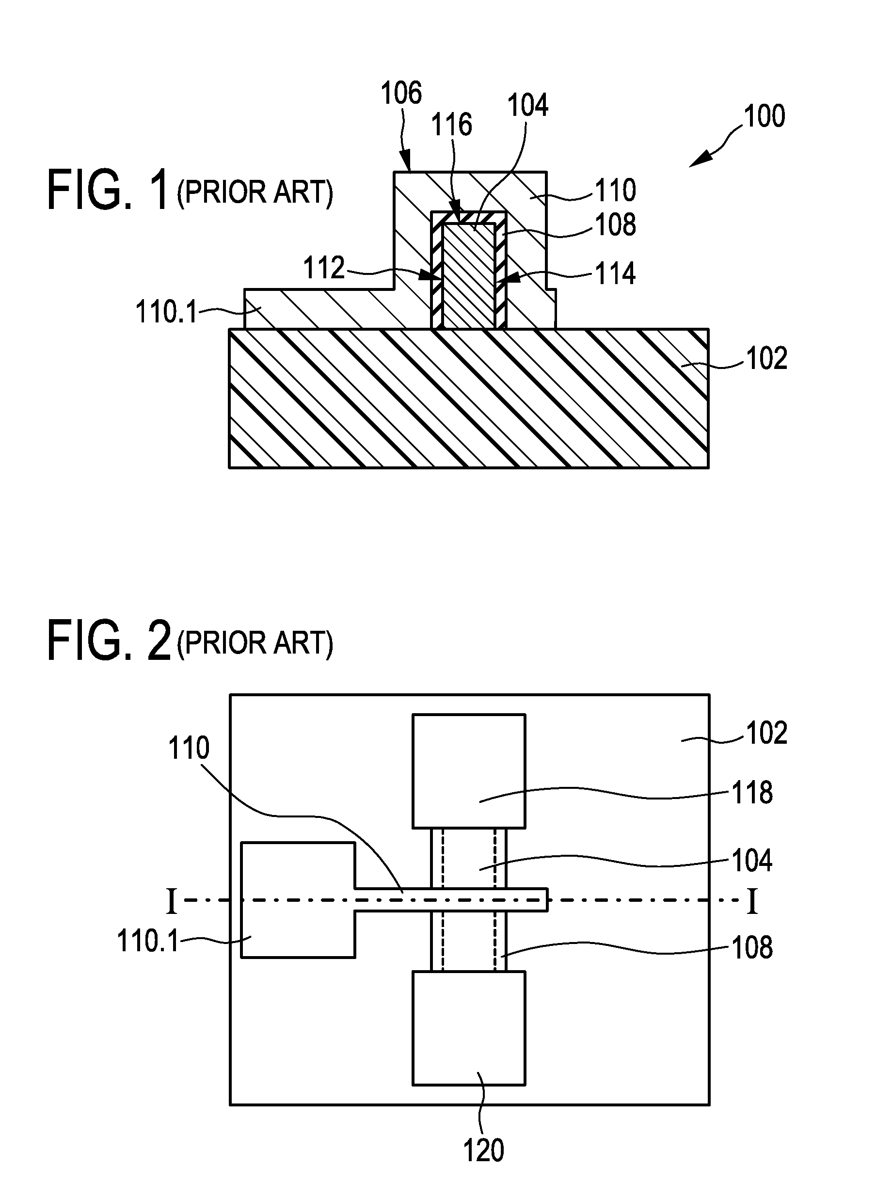
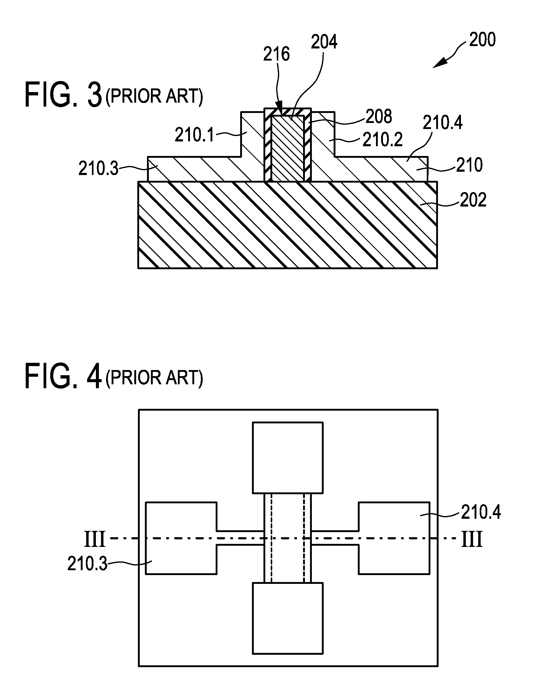
[0059]FIGS. 1 and 2 show a cross-sectional and a top view of a FinFET with a continuous gate stack according to the prior art. The cross-sectional view of FIG. 1 is taken along the broken line I-I in FIG. 2.

[0060]The FinFET structure 100 of the prior art is based on a substrate, typically a silicon-on-insulator (SOI) wafer. The FinFET structure builds on the originally buried insulator layer 102, which typically is made of silicon dioxide. At the processing stage shown in all the Figures, the surface silicon layer has been removed. A fin-shaped channel region 104, the fin of the FinFET 100, stands on a surface of the buried oxide layer 102. A gate stack 106 comprising a continuous first gate-isolation layer 108 and a continuous first gate layer 110 is arranged on the fin. The first gate-isolation layer 108 extends on mutually opposite lateral fin faces 112 and 114 and on a top fin face 116. The first gate layer 110 covers the first gate-isolation layer and laterally continues into a...


PUM


Abstract

The present invention relates to a FinFET with separate gates and to a method for fabricating the same. A dielectric gate-separation layer between first and second gate electrodes has an extension in a direction pointing from a first to a second gate layer that is smaller than a lateral extension of the fin between its opposite lateral faces. This structure corresponds with a processing method that starts from a covered basic FinFET structure with a continuous first gate layer, and proceeds to remove parts of the first gate layer and of a first gate-isolation layer through a contact opening to the gate layer. Subsequently, a replacement gate-isolation layer that at the same time forms the gate separation layer fabricated, followed by filling the tunnel with a replacement gate layer and a metal filling.

Description

FIELD OF THE INVENTION[0001]The present invention relates to a FinFET with separate gates and to a method for fabricating a FinFET with separate gates. It also relates to an integrated circuit comprising a FinFET and to a method for making the same.BACKGROUND OF THE INVENTION[0002]A FinFET is a transistor architecture of the metal-oxide-semiconductor field-effect transistor (MOSFET) type, which is favored as a replacement for planar MOSFET transistors in future integrated circuits fabricated in MOS technology, such as NMOS, PMOS, CMOS or BiCMOS.[0003]A FinFET comprises a gate structure, which is wrapped around three sides of a fin-shaped channel region that stands vertically on a substrate surface. The substrate surface is assumed as being oriented horizontally for the purpose of this description. In contrast to planar MOSFET transistors, which have a channel region in parallel orientation to the substrate surface, FinFETs allow superior channel charge control even at extremely shor...

Claims


Application Information

Patent Timeline
Patent Type & Authority Patents(United States)
IPC IPC(8): H01L21/3205
CPCH01L29/66545H01L29/66795H01L29/785H01L29/7856
Inventor SONSKY, JANSURDEANU, RADU
Owner UNITED MICROELECTRONICS CORP
Why Eureka
Try Eureka