Apparatus and method for inspecting substrate internal defects

a technology of internal defects and apparatus, applied in the field of apparatus and a method for inspecting internal defects of substrates, can solve the problems of reducing requiring a camera with a higher definition, and generating cracks on substrates, so as to improve the image definition of internal defects and improve the detection of internal defects

Inactive Publication Date: 2013-03-12
DELTA ELECTRONICS INC
View PDF11 Cites 2 Cited by
  • Summary
  • Abstract
  • Description
  • Claims
  • Application Information

AI Technical Summary

Benefits of technology

[0008]As a result, the present invention provides an illuminating method special designed for substrate inspection to resolve the above problems. The present invention uses the total reflection of light beam within a substrate to directly illuminate internal defects in the substrate so as to enhance the image definition of internal defects such as cracks, pores, impurities, bubbles, thickness difference and effectively avoid misidentifying foreign objects such as surface stains as internal defects. In addition to offering a more efficient capability to inspect internal defect, the method also can resolve the difficulty to inspect substrate internal defects after the substrate finished surface mount process.
[0011]Further, it is another objective of the present invention to provide an apparatus for inspecting substrate internal defects for receiving higher image definition of internal defects in a substrate.
[0013]The present invention renders light beam transmitting into a substrate and has a total reflection within the substrate where the light beam does not refract out of the substrate. When light beam is interfered by internal defects within the substrate, light beam moving path is changed. Such changes of light moving path result in reflection, refraction or scattering, and generate bright spots. Thus, the defect locations are detected by an image capturing module above the substrate. The method is effective in improving image definition of internal defects and offering higher detectability on internal defects

Problems solved by technology

In addition, cracks crack are generated on substrates because substrates undergo processes such as high temperature heating process and etching and are transported frequently in manufacturing processes.
Yet, when light intensity is higher than a certain level, light intensity of diffraction generated then becomes too strong which lowers the image definition of internal defects 12.
Thus, it is required to spend higher cost on a camera with higher definition to retrieve clear image.
In addition, under the circumstance when the tolerance of a substrate 10 is large, an optimal light intensity for retrieving the best image becomes a difficult decision.
Further, as shown in FIG. 3, when crack width of micro defects 12 under non parallel light becomes smaller, it is difficult to enhance image definition of micro crack by projecting light from different directions.

Method used


Image

  • Apparatus and method for inspecting substrate internal defects
  • Apparatus and method for inspecting substrate internal defects
  • Apparatus and method for inspecting substrate internal defects

Examples


Embodiment Construction

[0026]In cooperation with attached drawings, the technical contents and detailed description of the present invention are described thereinafter according to a preferable embodiment, being not used to limit its executing scope. Any equivalent variation and modification made according to appended claims is all covered by the claims claimed by the present invention.

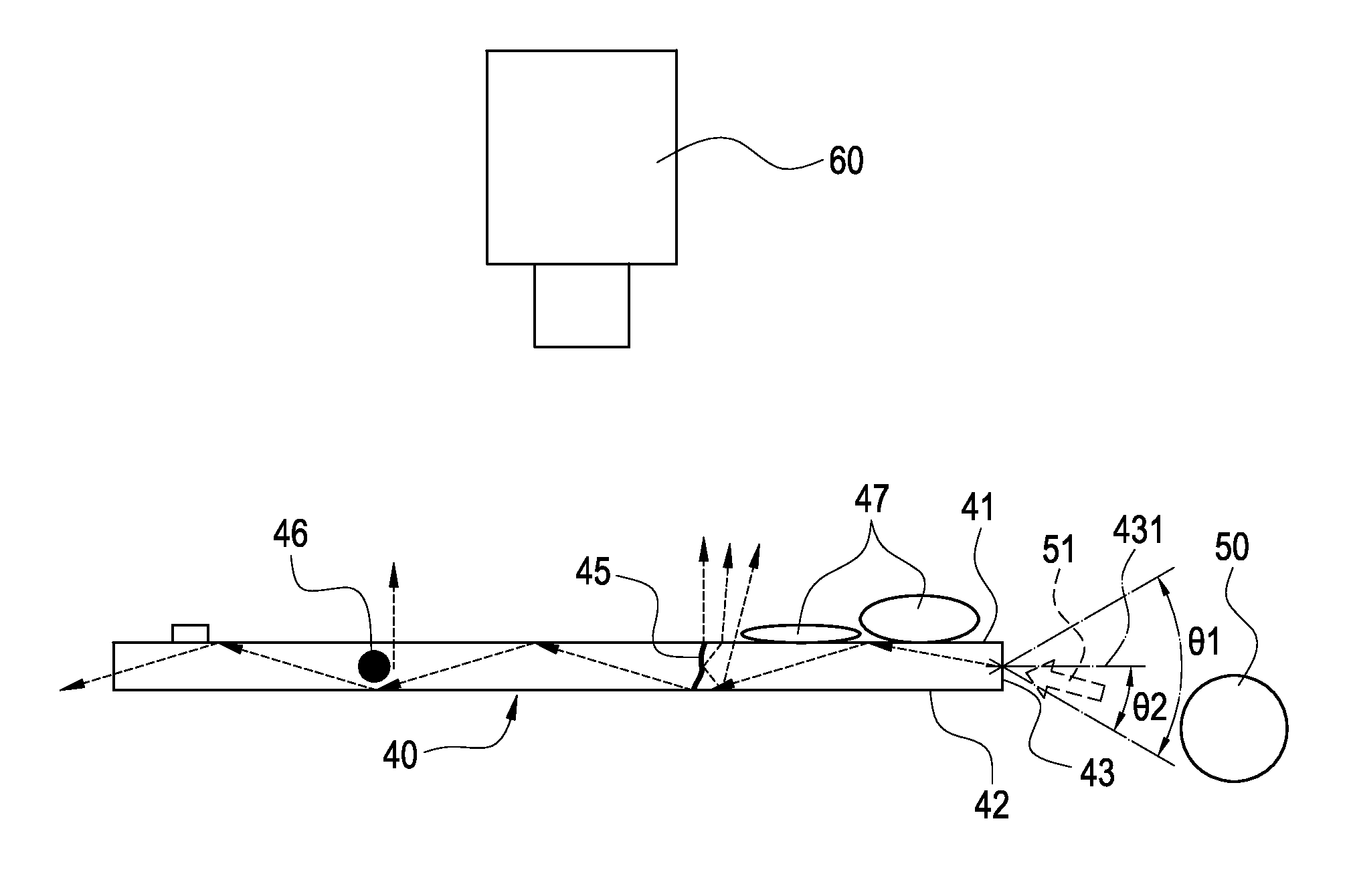
[0027]FIG. 4 is a schematic diagram of a preferred embodiment according to the present invention. The apparatus for inspecting substrate internal defects is suitable for use in internal defects inspection of a substrate 40. The apparatus for inspecting substrate internal defects mainly comprises a light source 50, and an image capturing module 60.

[0028]The light source 50 is disposed on one of the lateral sides 43 of the substrate 40 to emit a light beam 51 to the lateral side 43 for correspondingly penetrating the substrate 40. Preferably, the light beam emitted by the light source 50 moves along the same path to have stro...


PUM


Abstract

A method for inspecting substrate internal defects is disclosed. The method provides at least one light source disposed on a lateral side of a substrate and configured to emit a light beam to the lateral side for correspondingly penetrating the substrate. The method also provides an image capturing module for retrieving an image of the upper surface, wherein an incident angle of the light beam to the respective lateral side is limited within a first predetermined angle to allow the light beam to have a total reflection in the substrate. Thus, the light beam is blocked by internal defects when transmitting within the substrate to generate bright spots to be detected by the image capturing module for locating the defect position. The method provides a better image definition of internal defects images. The present invention further provides an apparatus based on the method for inspecting substrate internal defects.

Description

BACKGROUND OF THE INVENTION[0001]1. Field of the Invention[0002]The invention generally relates to an apparatus and a method for inspecting substrate internal defects.[0003]2. Description of Prior Art[0004]Semiconductor manufacturing processes such as thin film deposition are used for fabricating electronic components on a substrate. Accordingly, the quantity of internal defects in the substrate such as inclusions, bubbles, cracks is a critical factor indicating the quality of electronic components. In addition, cracks crack are generated on substrates because substrates undergo processes such as high temperature heating process and etching and are transported frequently in manufacturing processes.[0005]Thus, inspecting internal defects on a substrate is an indispensable non destructive inspection. At present, the most frequently used crack inspection method arranges illuminating light sources beneath the substrate to emit light beam towards the lower surface of the substrate and pe...

Claims


Application Information

Patent Timeline
Patent Type & Authority Patents(United States)
IPC IPC(8): G06K9/00
CPCG01N21/9505
Inventor CHANG, JEN-MINGLEE, YU-HSICHOU, YEN-CHUNCHEN, CHENG-KAILIN, JUI-YU
Owner DELTA ELECTRONICS INC
Why Eureka
Try Eureka