

Package structure having MEMS elements and fabrication method thereof
a technology of microelectromechanical system and packaging structure, which is applied in the direction of fluid pressure measurement, instrumentation, and semiconductor/solid-state device details, can solve the problems of large size of packaging structure, high degree of accuracy, and high cost of tsv technology for forming through holes and recesses, so as to reduce equipment and fabrication costs, reduce the overall thickness and size of the package structure, and reduce the effect of at least one round of exposur
- Summary
- Abstract
- Description
- Claims
- Application Information
AI Technical Summary
Benefits of technology
Problems solved by technology
Method used
Image

Examples
Embodiment Construction
[0017]The following illustrative embodiments are provided to illustrate the disclosure of the present invention and its advantages, these and other advantages and effects being apparent to those in the art after reading this specification.
[0018]It should be noted that the drawings are only for illustrative purposes and not intended to limit the present invention. Meanwhile, terms such as ‘up’, ‘down’, ‘a’ and so on are used as a matter of descriptive convenience and not intended to have any other significance or provide limitations for the present invention.
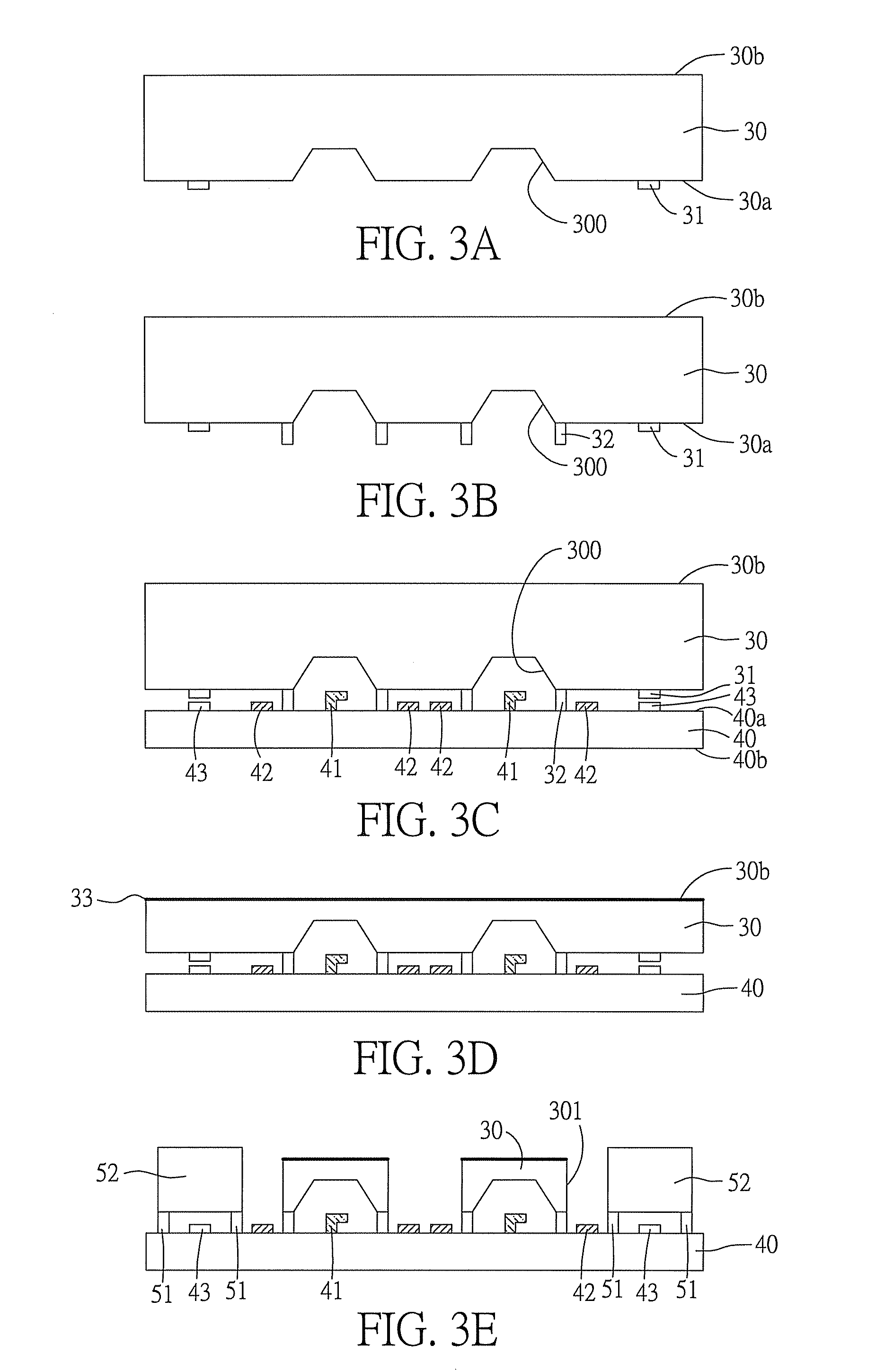
[0019]FIGS. 3A to 3K show a fabrication method of a package structure having MEMS elements according to the present invention. Therein, FIG. 3E′ is a top view of FIG. 3E, and FIG. 3J′ is another embodiment of FIG. 3J.
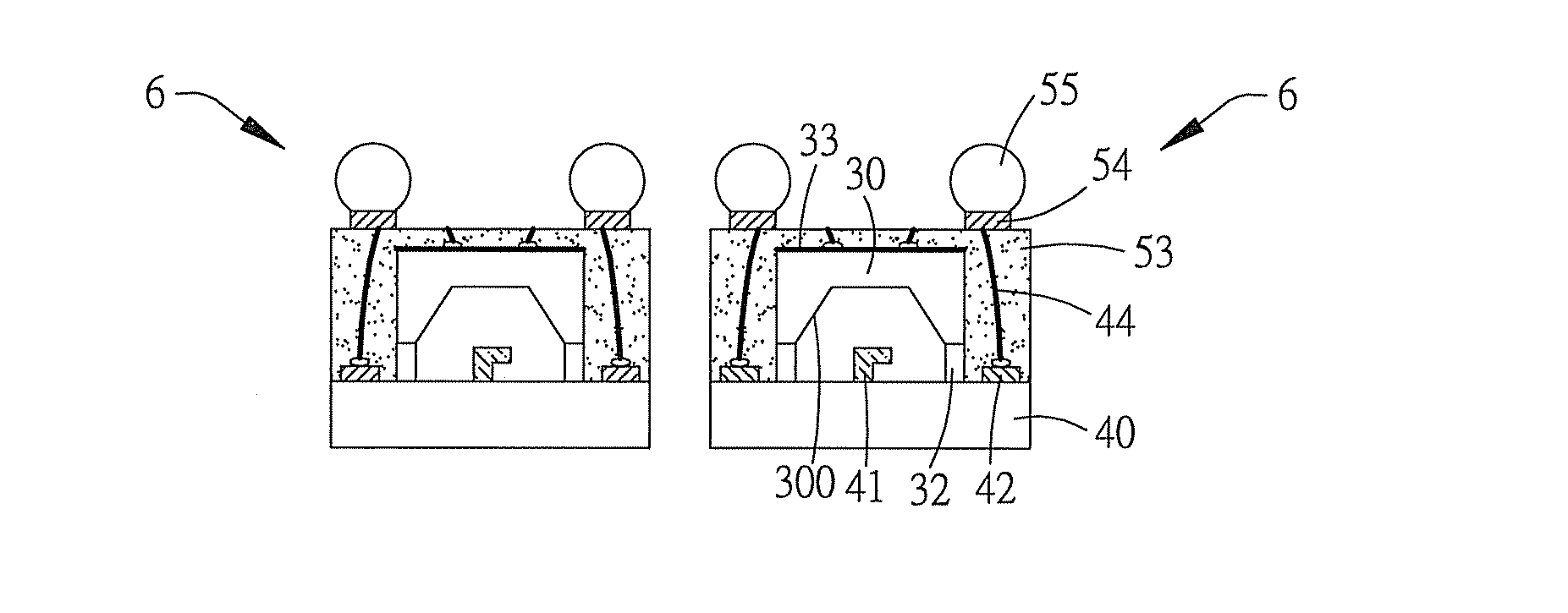
[0020]Referring to FIG. 3A, a plate 30 having a first surface 30a with a plurality of first alignment keys 31 and a second surface 30b opposite to the first surface 30a is provided. The plate 30 can be a silicon-cont...
PUM
 Abstract
Description
Claims
Application Information