Mach-zehnder waveguide type optical modulator

a waveguide and optical modulator technology, applied in non-linear optics, instruments, optics, etc., can solve problems such as a variation in bias point, a decrease in extinction ratio, and a decrease in optical loss, so as to reduce the extinction ratio, suppress the optical loss, and shorten the part of the optical waveguide

Active Publication Date: 2013-03-26
SUMITOMO OSAKA CEMENT CO LTD
View PDF20 Cites 6 Cited by
  • Summary
  • Abstract
  • Description
  • Claims
  • Application Information

AI Technical Summary

Benefits of technology

[0022]According to the configuration described in the first aspect of the invention, the Mach-Zehnder waveguide type optical modulator includes the thin plate with a thickness of 20 μm or less formed of a material having an electro-optical effect, the optical waveguide formed on a front surface or a rear surface of the thin plate, and the modulation electrode modulating light passing through the optical waveguide, wherein the optical waveguide includes an input optical waveguide, branched optical waveguides, and an output optical waveguide, wherein the branched optical waveguide includes an input branching portion in which the input optical waveguide is branched into a plurality of optical waveguides, an output merging portion in which the plurality of optical waveguides connected to the output optical waveguide is merged, and a parallel portion formed between the input branching portion and the output merging portion, and wherein at least one of the input branching portion and the output merging portion has a ratio lid of a length l along a symmetry axis of the branched optical waveguides to a gap d of the optical waveguide in the parallel portion in the range of 33 to 100. Accordingly, for example, when a Mach-Zehnder waveguide with an optical waveguide gap d of 30 μm is formed, the length l of the input branching portion or the output merging portion along the symmetry axis of the branched optical waveguides was 4 mm in the past, which is about 120 times the optical waveguide gap d, but can be reduced to 1 mm in the invention. By this reduction, it is possible to further shorten the part of the optical waveguide which is influenced by the photorefractive phenomenon or in which stray light is coupled to signal light. In addition, it is possible to suppress the optical loss due to the stray light in that part or the decrease in extinction ratio.
[0023]By employing this configuration, it is also possible to reduce the entire size of the Mach-Zehnder waveguide type optical modulator.
[0024]According to the configuration described in the second aspect of the invention, since the curved portion of the optical waveguide in at least one of the input branching portion and the output merging portion has a minimum radius of curvature R of 0.2 to 100 mm, it is possible to reduce the length l of the input branching portion or the output merging portion along the symmetry axis of the branched optical waveguides. Particularly, when the gap between two branched waveguides of the Mach-Zehnder waveguide is enlarged to prevent the crosstalk, it is possible to effectively reduce the length l.
[0025]According to the configuration described in the third aspect of the invention, since at least a part of the parallel portion includes a curved portion and the curved portion has a minimum radius of curvature R of 0.2 to 100 mm, it is possible to reduce the length of the parallel portion (the distance between the start point and the end point of the parallel portion), as well as the input branching portion or the output merging portion. Accordingly, it is possible to suppress the influence of the photorefractive phenomenon or the coupling of stray light to signal light and to reduce the size of the optical modulator.
[0026]According to the configuration described in the fourth aspect of the invention, since a part of the optical waveguide has a ridge structure, it is possible to enlarge the difference in refractive index between the optical waveguide and the periphery thereof and thus to improve the confinement of light in the curved portion. Accordingly, it is possible to suppress leakage from the curved portion of the optical waveguide and to sufficiently satisfy the conditions such as the relation of the above-mentioned ratio l / d or the minimum radius of curvature R.
[0027]According to the configuration described in the fifth aspect of the invention, since the ridge structure is formed in at least a part of the optical waveguide having a minimum radius of curvature, it is possible to effectively suppress the leakage of light from the part having the minimum radius of curvature. Accordingly, it is possible to make the optical waveguide compact and it is also possible to not only suppress the influence of the photorefractive phenomenon or the coupling of stray light to signal light, but to reduce the generation of stray light itself as the cause thereof.

Problems solved by technology

However, in a wide-bandwidth optical modulator, for example, an optical modulator corresponding to 40 GHz, when the optical input power input to the optical modulator is enhanced for the purpose of transmission over a long distance, problems occur such as a decrease in extinction ratio, an increase in optical loss, and a variation in bias point.
Particularly, when the optical input power is equal to or greater than 10 mW, these problems become marked.
As a result of extensive research, the inventors found that the problems are caused by signal light propagating in the optical waveguide interfering with stray light generated in an input portion for inputting a laser beam to the optical modulator, the optical waveguide in the optical modulator causing a photorefractive phenomenon, and a grating being formed in the optical waveguide portion.
On the other hand, when the thickness of the substrate is set to 30 μm or less or 20 μm or less as in Patent Citations 1 and 2, the density of the stray light confined in the substrate increases and it is thus not possible to satisfactorily suppress the deterioration in characteristics of the optical modulator such as the decrease in extinction ratio and the increase in optical loss only by the use of the stray light removing means described in Patent Citation 3, compared with the optical waveguide type modulator with a thickness of a substrate of about 1 to 0.5 mm.
Accordingly, reduction of the influence of the photorefractive phenomenon on the Mach-Zehnder waveguide type optical modulator is an important issue.

Method used


Image

  • Mach-zehnder waveguide type optical modulator
  • Mach-zehnder waveguide type optical modulator
  • Mach-zehnder waveguide type optical modulator

Examples


example 1

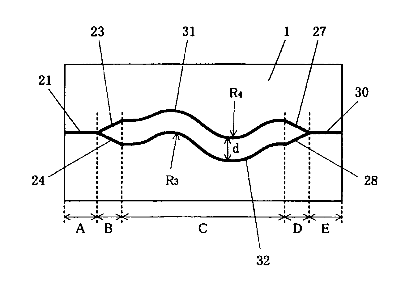
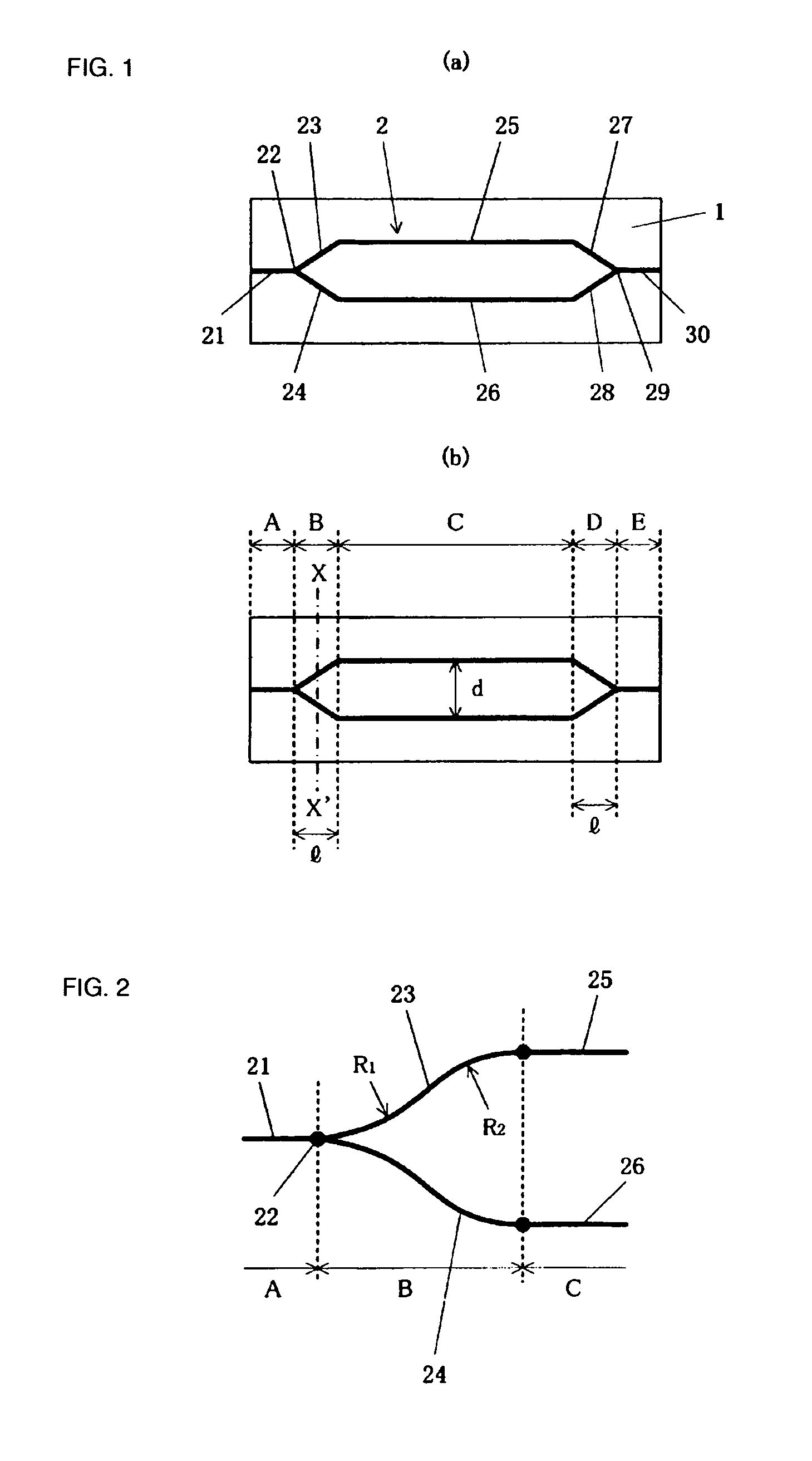
[0061]In an optical modulator according to Example 1, an X-cut LN substrate with a thickness of 500 μm is used as a substrate and an optical waveguide is formed on the surface of the substrate using a Ti diffusion process. The shape of the Mach-Zehnder optical waveguide shown in FIG. 1 is employed as the shape of the optical waveguide. The lengths of the input optical waveguide 21 and the output optical waveguide 30 are about 5 mm, the lengths l of the input branching portion (region B) and the output merging portion (region D) along the symmetry axis are about 3 mm, the length of the parallel portion (region C) is 30 mm, and the gap d between the branched waveguides in the parallel portion is 30 μm. The minimum radius of curvature R in regions B and D is set to 100 mm.

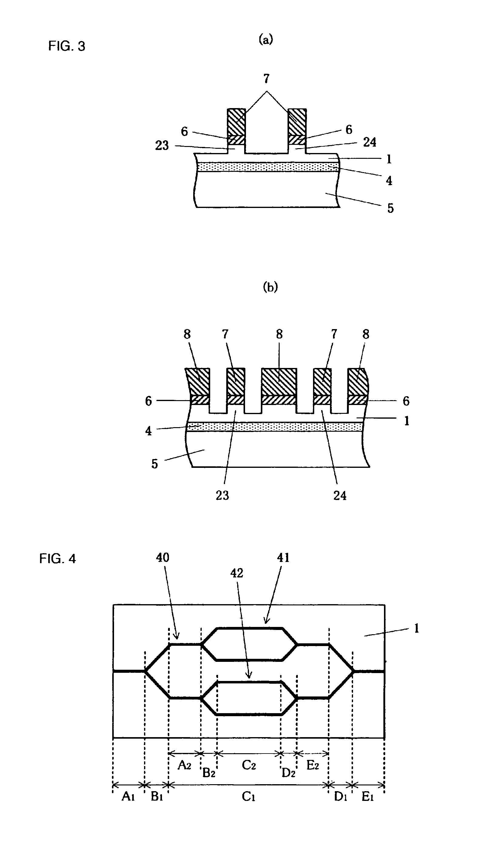
[0062]Then, the rear surface of the substrate is ground until the thickness of the substrate becomes 10 μm, and is bonded to a reinforcement plate using a UV-curable adhesive as an adhesive layer. The modulation elect...

examples 2 to 4

[0063]In Examples 2 to 4, a Mach-Zehnder waveguide type optical modulator is formed in the same way as Example 1 except that the length l, the gap d between the branched waveguides, and the minimum radius of curvature R in Example 1 are changed as shown in Table 1.

example 5

[0064]In an optical modulator according to Example 5, a Z-cut LN substrate with a thickness of 500 μm is used as a substrate and an optical waveguide is formed on the surface of the substrate using a Ti diffusion process. Then, the rear surface of the substrate is ground by the use of a grinder until the thickness of the substrate becomes 5 μm, and is bonded to a reinforcement plate using a UV-curable adhesive as an adhesive layer. The shape of the Mach-Zehnder optical waveguide shown in FIG. 1 is employed as the shape of the optical waveguide. The lengths of the input optical waveguide 21 and the output optical waveguide 30 are about 4 mm, the lengths l of the input branching portion (region B) and the output merging portion (region D) along the symmetry axis are about 0.825 mm, the length of the parallel portion (region C) is 35 mm, the gap d between the branched waveguides in the parallel portion is 25 μm, and the minimum radius of curvature R is 0.2 mm. The optical waveguides of...


PUM

PropertyMeasurementUnit
thicknessaaaaaaaaaa
thicknessaaaaaaaaaa
thicknessaaaaaaaaaa

Abstract

It is intended to suppress the influence of a photorefractive phenomenon or the coupling of stray light to signal light. A Mach-Zehnder waveguide type optical modulator is provided which includes a thin plate 1 with a thickness of 20 μm or less formed of a material having an electro-optical effect, an optical waveguide 2 formed on a front surface or a rear surface of the thin plate, and a modulation electrode modulating light passing through the optical waveguide. The optical waveguide includes an input optical waveguide 21, branched optical waveguides 23 to 28, and an output optical waveguide 30. The branched optical waveguide includes an input branching portion (region B) in which the input optical waveguide is branched into a plurality of optical waveguides, an output merging portion (region D) in which the plurality of optical waveguides connected to the output optical waveguide are merged, and a parallel portion (region C) formed between the input branching portion and the output merging portion. At least one of the input branching portion and the output merging portion has a ratio l / d of a length l along a symmetry axis of the branched optical waveguides to a gap d of the optical waveguide in the parallel portion in the range of 33 to 100.

Description

TECHNICAL FIELD[0001]The present invention relates to a Mach-Zehnder waveguide type optical modulator, and more particularly, to a Mach-Zehnder waveguide type optical modulator including a thin plate with a thickness of 20 μm or less formed of a material having an electro-optical effect.BACKGROUND ART[0002]In the fields of optical communications or optical measurements, optical modulators have been widely used. Particularly, with the development of multimedia, the amount of information being transmitted tends to increase and there is a demand for enlargement in the modulation frequency bandwidth of optical modulators. As one means for fulfilling the demand, an external modulation system as a waveguide type optical modulator in which an optical waveguide or a modulation electrode is formed on a substrate formed of lithium niobate (LN) or the like having an electro-optical effect has been employed and the diversification thereof has proceeded. For the purpose of the enlargement in fre...

Claims


Application Information

Patent Timeline
Patent Type & Authority Patents(United States)
IPC IPC(8): G02F1/035
CPCG02F1/225G02F2001/212G02F2201/063G02F1/212
Inventor OIKAWA, SATOSHIKONDOU, KATSUTOSHIICHIOKA, MASAYUKI
Owner SUMITOMO OSAKA CEMENT CO LTD
Why Eureka
Try Eureka