Image processing device and associated methodology of processing gradation noise

a technology of image processing and noise reduction, applied in the field of image processing, can solve the problem of poor denoising performance of images with gradation

Inactive Publication Date: 2013-04-02
SONY CORP
View PDF8 Cites 35 Cited by
  • Summary
  • Abstract
  • Description
  • Claims
  • Application Information

AI Technical Summary

Benefits of technology

[0016]Thus, it is desirable to provide an image processing device, an image processing method, a program, and an imaging device each achieving excellent denoising performance.
[0021]According to the embodiments of the present invention, an optimal estimated plane having the least error between the luminance values of the respective pixel in the block and the luminance values in an estimated plane is determined and the weighting factor for the reference pixel is calculated on the basis of the luminance value of the reference pixel and a luminance value in the optimal estimated plane. Hence, not only is it possible to achieve denoising of a gradation portion that has been unfeasible in the related art, but it is also possible to preserve a detailed portion (edge or the like) of the image data.

Problems solved by technology

The techniques described above, however, have a problem that denoising performance is poor for an image having gradation (a region in which the luminance varies in a planer manner).

Method used


Image

  • Image processing device and associated methodology of processing gradation noise
  • Image processing device and associated methodology of processing gradation noise
  • Image processing device and associated methodology of processing gradation noise

Examples


Embodiment Construction

[0028]Hereinafter, embodiments of the present invention will be described specifically with reference to the drawings in the following order.

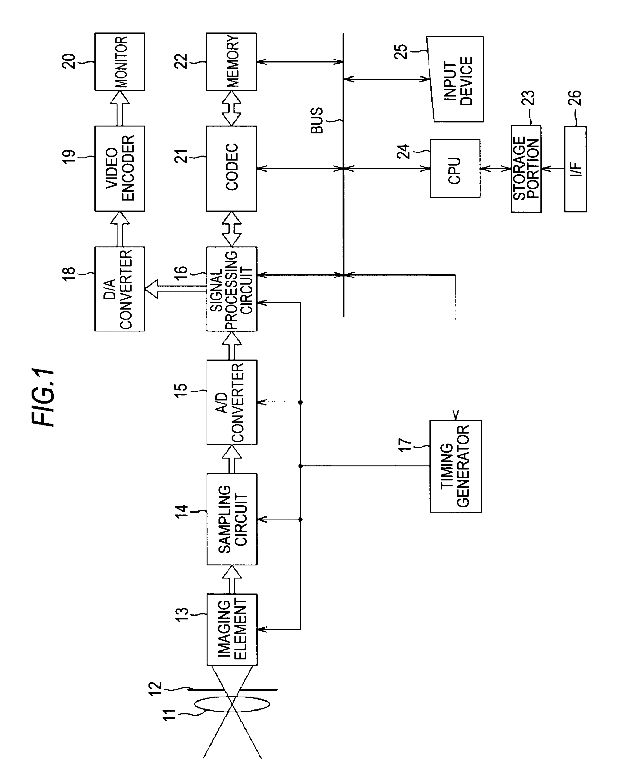
[0029]1. Camera configuration with reference to FIG. 1

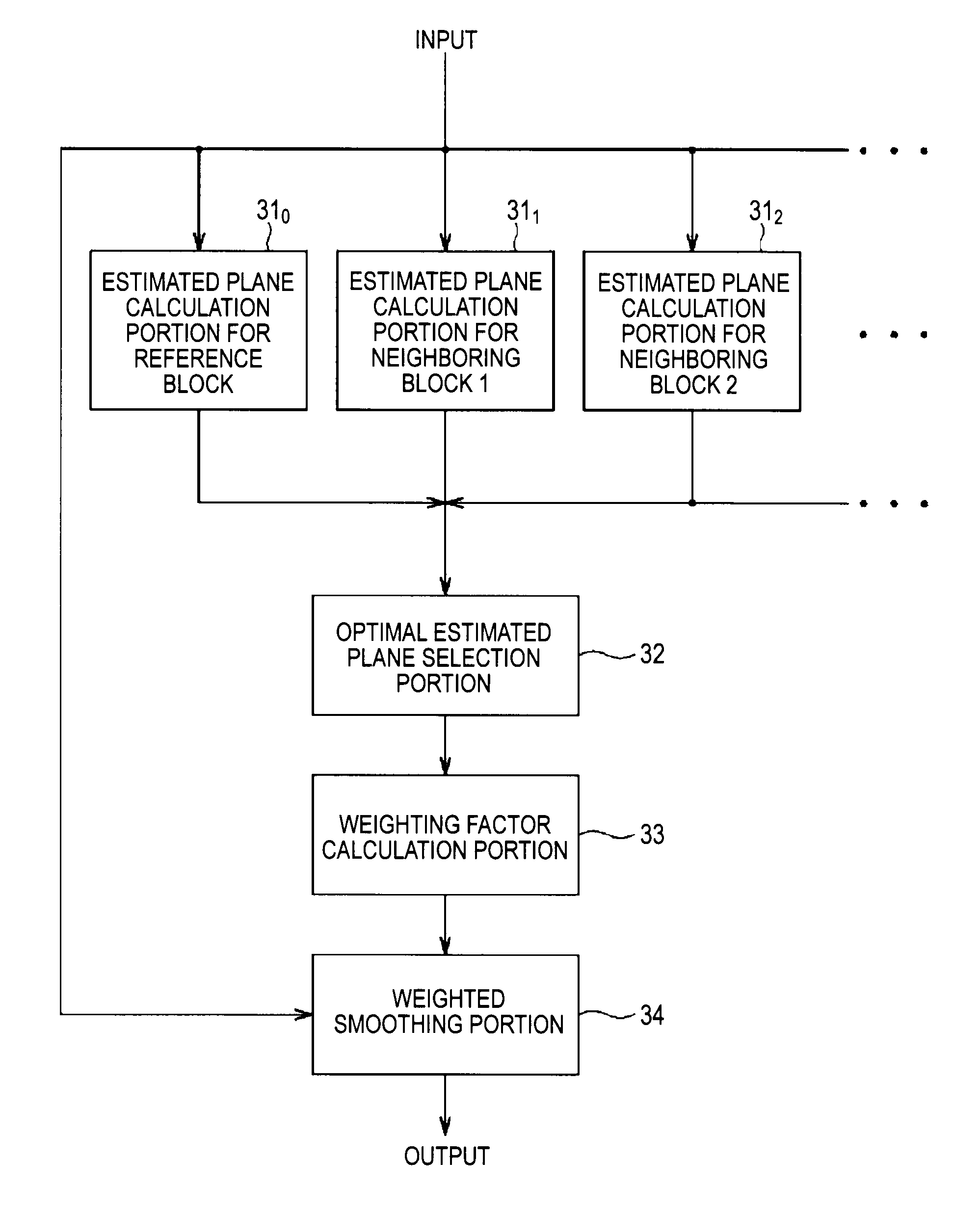
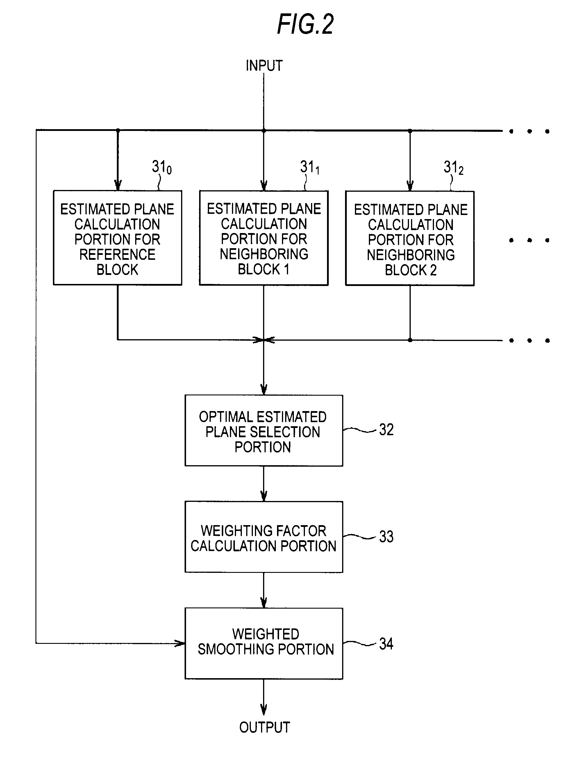
[0030]2. Image processing example 1 with reference to FIG. 2 through FIG. 5C

[0031]3. Image processing example 2

[0032]4. Modification with reference to FIG. 6

1. Camera Configuration

[0033]FIG. 1 shows an example of a camera configuration according to an embodiment of the present invention. Light from a subject is collected onto an imaging element 13 by an optical system, such as a lens 11 and an aperture 12.

[0034]The imaging element 13 is formed, for example, of a CCD (Charge Coupled Device), a CMOS (Complementary Metal Oxide Semiconductor) imager, or the like. It converts received light into an electric signal and outputs the electric signal to a correlated double sampling circuit 14. More specifically, the imaging element 13 receives light coming from the subject via the lens 11 and the aper...


PUM


Abstract

An image processing device includes: an estimated plane calculation portion calculating, for inputted image data, estimated planes defined by luminance values in blocks each containing a predetermined number of pixels including a reference pixel; an optimal estimated plane selection portion selecting an optimal estimated plane having a least summation of errors between luminance values of respective pixels in a block and an estimated plane among the estimated planes; a weighting factor calculation portion calculating a weighting factor for the reference pixel base on luminance values of the reference pixel and in the optimal estimated plane; and a weighted smoothing portion computing a sum of products of relative luminance differences between the luminance values of the respective pixels in the block and in the optimal estimated plane and the weighting factor for the reference pixel and adding a luminance value in the optimal estimated plane at a reference pixel position to a result of computation.

Description

BACKGROUND OF THE INVENTION[0001]1. Field of the Invention[0002]The present invention relates to image processing that applies denoising to image data having noises.[0003]2. Description of Related Art[0004]A widespread use of digital cameras in recent years makes it necessary to restore a digital image often taken under unfavorable conditions. In particular, an image taken at low-light intensity like in night time has noises because an amount of light inputted into the camera is small. For example, in the case of a nightwatch camera, influences of noises make it difficult to discriminate the face of an individual or a vehicle license plate number to be subjected to surveillance. In order to overcome this inconvenience, a scheme to remove a noise from an image having noises is necessary. Such a scheme is achieved by a technique generally referred to as noise reduction.[0005]The purpose of noise reduction is to remove noises. It is, however, also desirable to preserve a detailed porti...

Claims


Application Information

Patent Timeline
Patent Type & Authority Patents(United States)
IPC IPC(8): G06K9/40G09G5/10G09G1/14G09G3/30G09G5/00G09G5/02G09G3/28H04N1/40H04N5/00H04N5/202H04N9/64G06T5/00H04N5/217H04N5/225H04N5/243
CPCG06T5/004H04N5/357G06T2207/20201H04N25/60
Inventor HAMADA, TAKEHIROTSUNASHIMA, NOBUHIRO
Owner SONY CORP
Why Eureka
Try Eureka