

Electronic device, conductive composition, metal filling apparatus, and electronic device manufacturing method
a technology of electronic devices and metal filling, which is applied in the direction of soldering apparatus, inorganic insulators, conductors, etc., can solve the problems of high power consumption of electronic devices, difficult to achieve compactification, and increase in wiring length,
- Summary
- Abstract
- Description
- Claims
- Application Information
AI Technical Summary
Benefits of technology
Problems solved by technology
Method used
Image

Examples
first embodiment
(1) First Embodiment
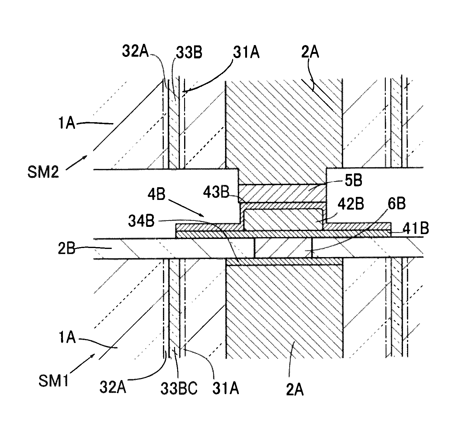
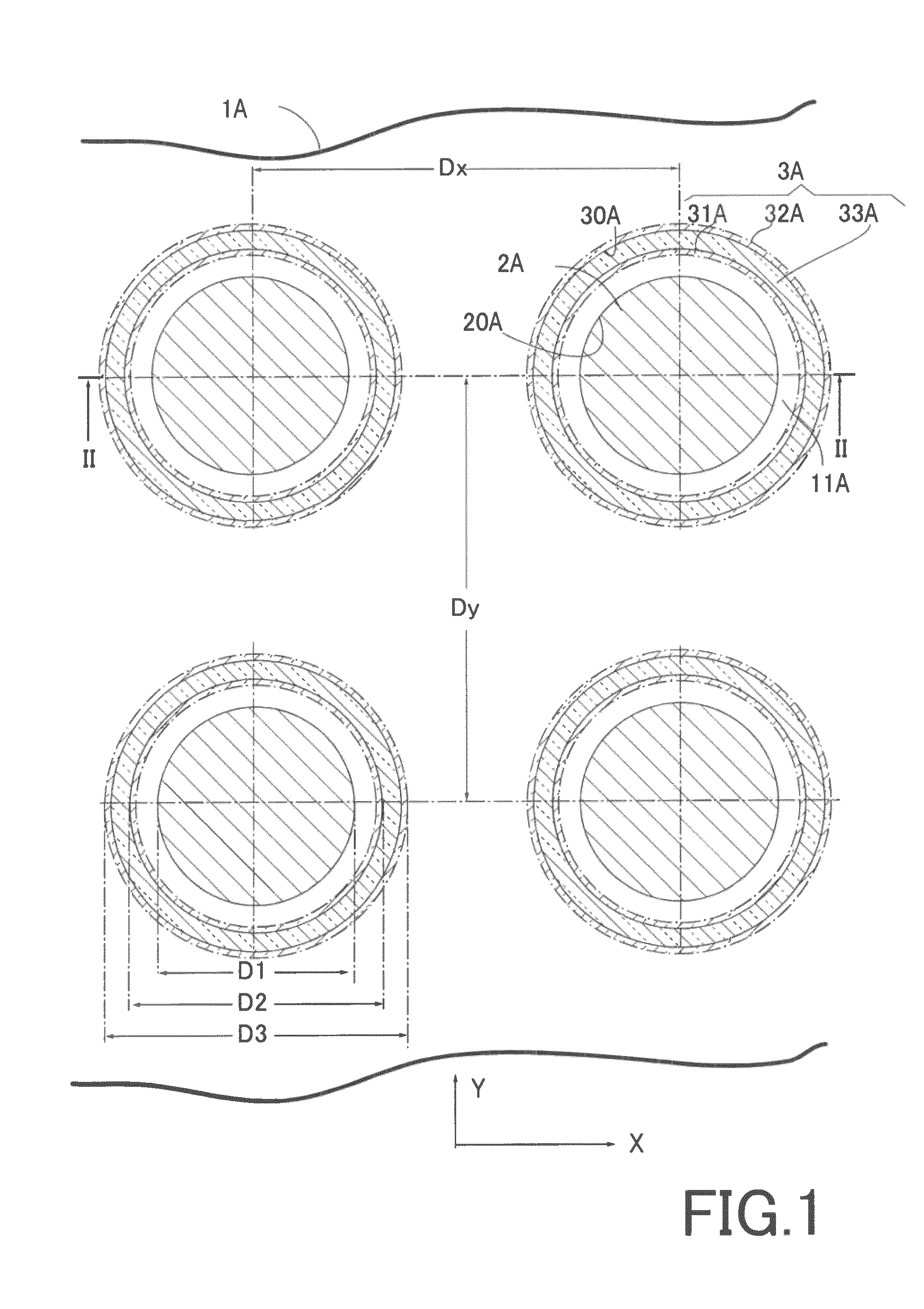
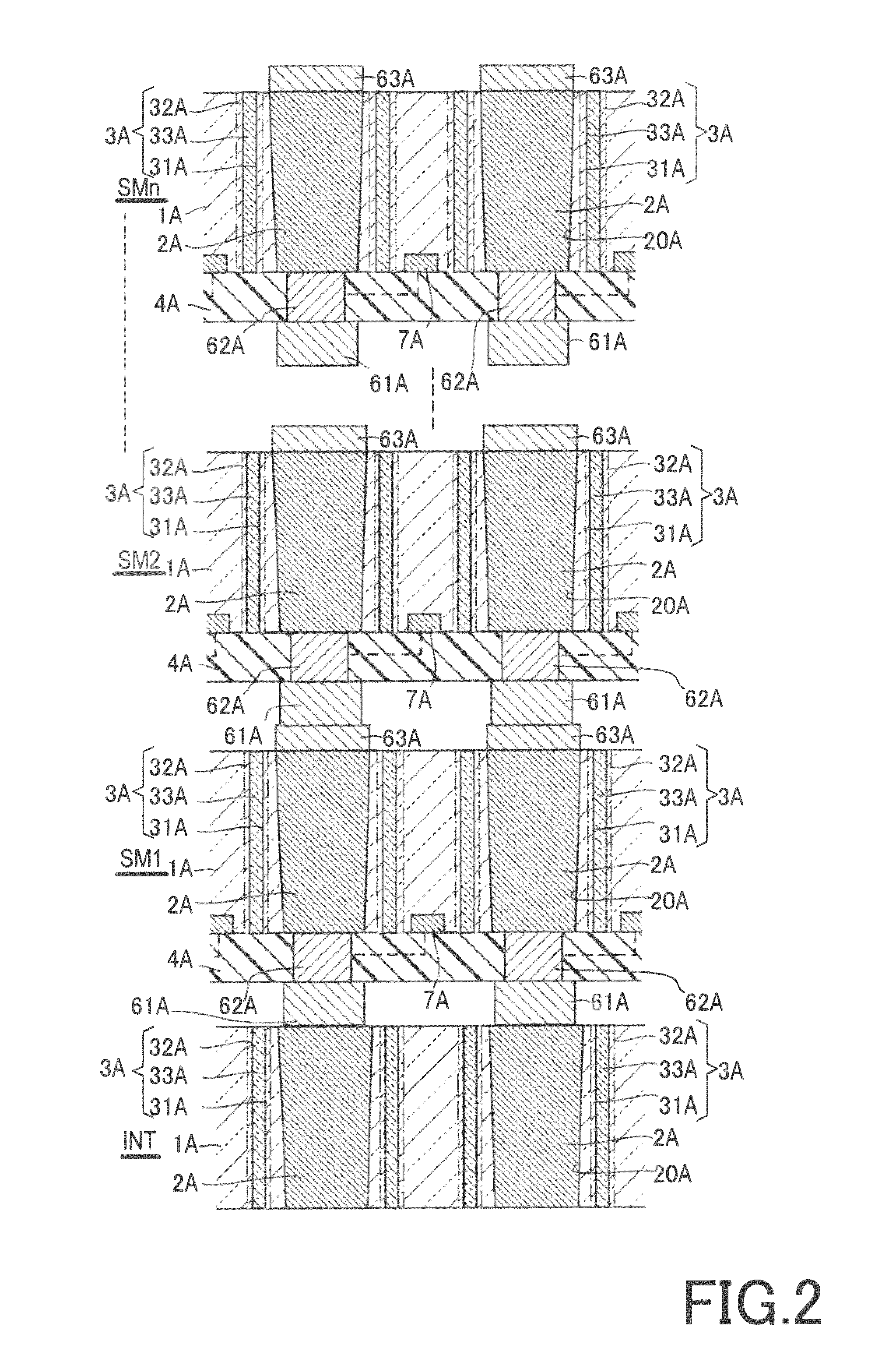
[0220]Referring to FIG. 17, a columnar conductor 3 fills a minute space 30 extending along the thickness direction from one surface of a substrate 1. At the bottom of the minute space 30, one end of the columnar conductor 3 is opposed to a film surface of a first conductor 2 across a junction film 4.
[0221]Although FIG. 17 illustrates the case where a single columnar conductor 3 is provided for a single first conductor 2, it should not be construed as limited thereto. It is also possible to provide a plurality of columnar conductors 3 for a single first conductor 2.
[0222]The minute space 30 filled with the columnar conductor 3 is a through-hole, a non-through-hole (blind hole), or a via hole. While the minute space 30 has a hole diameter of, for example, 60 μm or less, the thickness of the wafer itself is typically tens of μm. Accordingly, the minute space 30 has a considerably high aspect ratio.
[0223]Referring to FIG. 17, the first conductor 2 is formed flat on t...
second embodiment
(2) Second Embodiment
[0237]FIG. 25 is a view showing another embodiment of a substrate to be used for an electronic device according to the present invention. The present embodiment is characterized in that the junction film 4 is joined to almost the entire peripheral surface of the columnar conductor 3 within the minute space 30. The junction film 4 may be formed by a thin-film formation technology such as sputtering.
[0238]In the embodiment shown in FIG. 25, since the metal element contained in the junction film 4 is diffused into the columnar conductor 3 to create the alloy area AL over the entire peripheral surface of the columnar conductor 3, mutual junction strengths between the first conductor 2, the columnar conductor 3 and the substrate 1 can be further increased in comparison with the embodiment shown in FIG. 17.
[0239]Next will be described a method for manufacturing the substrate shown in FIG. 25.
A. Manufacturing Method 1
[0240]For example, after the minute space 30 is form...
PUM
| Property | Measurement | Unit |
|---|---|---|
| thickness | aaaaa | aaaaa |
| aspect ratio | aaaaa | aaaaa |
| diameter | aaaaa | aaaaa |
Abstract
Description
Claims
Application Information