Structure for flash memory cells

a technology of flash memory cells and structures, applied in the direction of semiconductor devices, electrical apparatus, transistors, etc., can solve the problems of increased leakage current and/or/, difficulty in achieving uniformity, etc., to improve induced reverse tunneling voltage failure, improve quality, and improve the effect of uniformity

Active Publication Date: 2013-05-21
TAIWAN SEMICON MFG CO LTD
View PDF26 Cites 9 Cited by
  • Summary
  • Abstract
  • Description
  • Claims
  • Application Information

AI Technical Summary

Benefits of technology

[0011]An advantage of an embodiment is that a high quality oxide spacer with good uniformity is provided to improve induced reverse tunneling voltage failure by widening process window, and an additional isolation layer is provided to improve leakage current performance.
[0012]A further advantage of an embodiment is that existing fabrication processes may be used with minor modification to several etching and layer deposition steps. This leads to simple implementation with small incurred costs.
[0013]Yet another advantage of an embodiment is that the elimination of a sharp point in a floating gate may help to reduce electric field intensification, which may reduce program function failures and increase yield.

Problems solved by technology

However, spacer 205 formed solely from an oxide layer may be prone to damage from other fabrication process steps and uniformity may be difficult to achieve with an oxide layer alone.
Sharp point 215, resulting from a poly etch, may lead to increased leakage current and / or induced reverse tunneling voltage failure.

Method used


Image

  • Structure for flash memory cells
  • Structure for flash memory cells
  • Structure for flash memory cells

Examples


Embodiment Construction

[0023]The making and using of the embodiments are discussed in detail below. It should be appreciated, however, that the present invention provides many applicable inventive concepts that can be embodied in a wide variety of specific contexts. The specific embodiments discussed are merely illustrative of specific ways to make and use the invention, and do not limit the scope of the invention.

[0024]The embodiments will be described in a specific context, namely flash memory structures and methods of forming same. The intermediate stages of manufacturing preferred embodiments are illustrated. Throughout the various views and illustrative embodiments, like reference numbers are used to designate like elements.

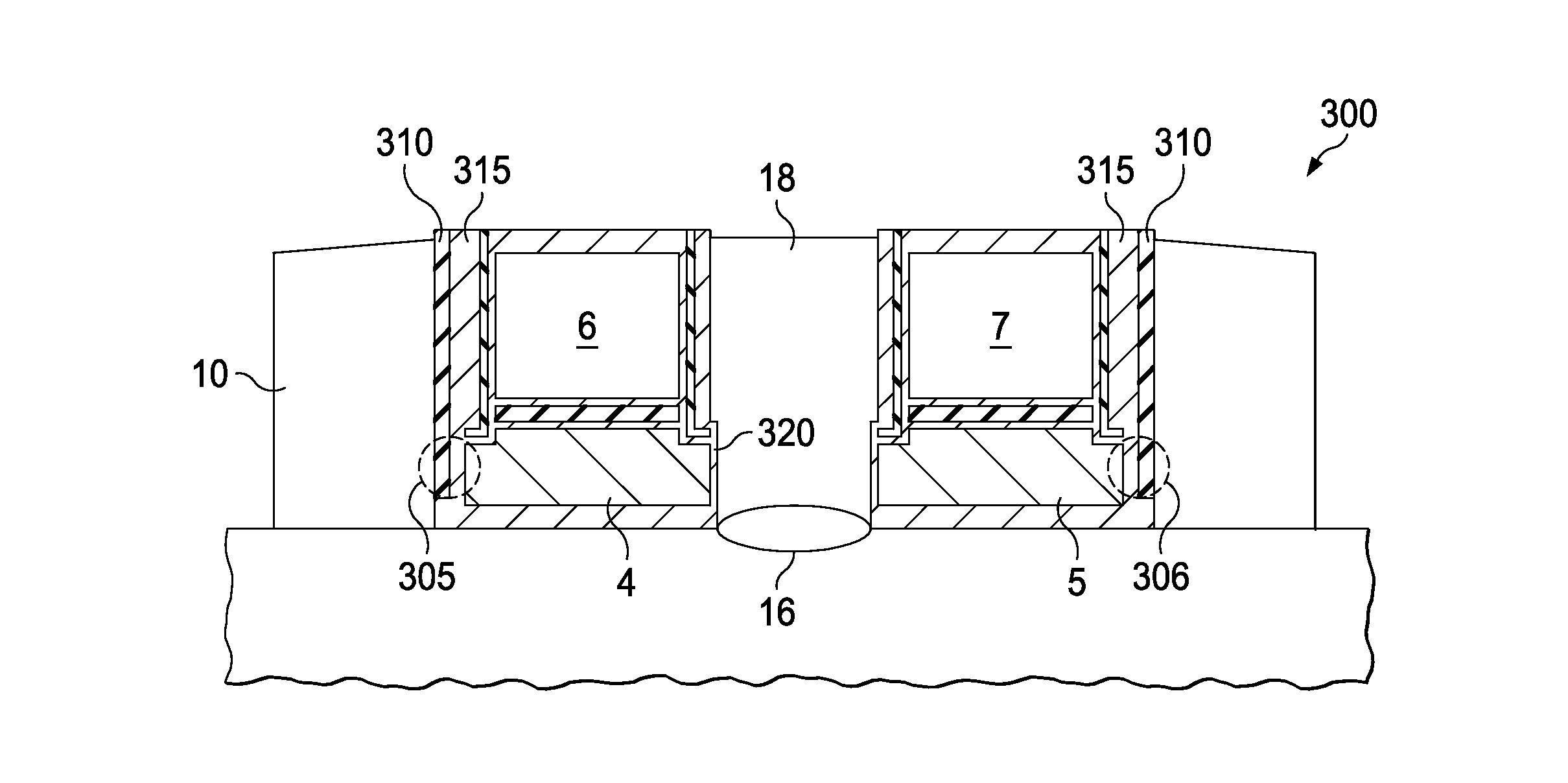
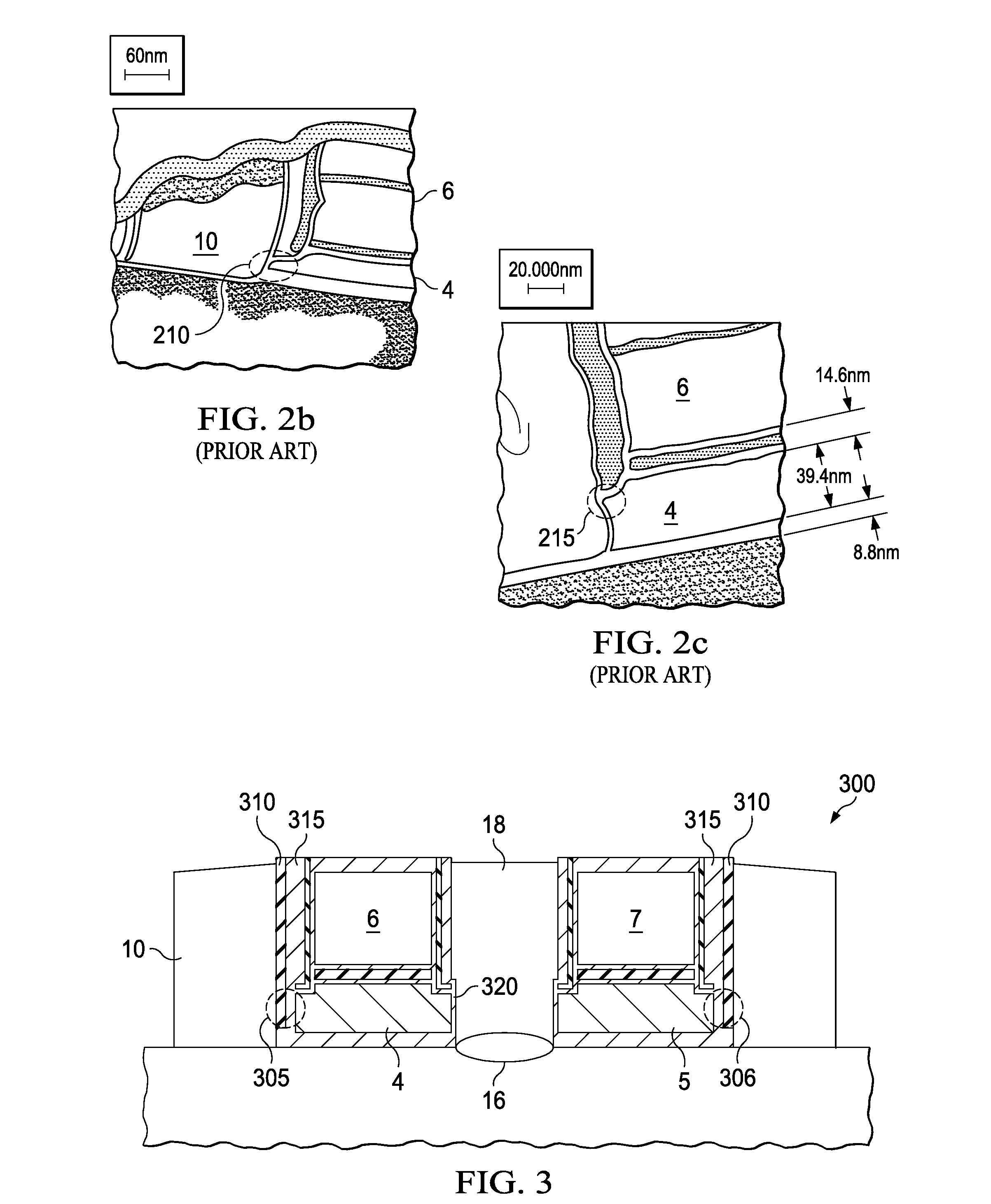
[0025]FIG. 3 illustrates a cross-sectional view of a structure 300 of flash memory cells. Structure 300 of flash memory cells displays an enhanced spacer 305 between word-line 10 and floating gate 4. Enhanced spacer 305 comprises an isolation layer 310 and an oxide layer 315, wher...


PUM


Abstract

A flash memory cell structure is provided. A semiconductor structure includes a semiconductor substrate, a floating gate overlying the semiconductor substrate, a word-line adjacent to the floating gate, an erase gate adjacent to a side of the floating gate opposite the word-line, a first sidewall disposed between the floating gate and the word-line, and a second sidewall disposed between the floating gate and the erase gate. The first sidewall has a first characteristic and the second sidewall has a second characteristic. The first characteristic is different from the second characteristic.

Description

[0001]This application claims the benefit of U.S. Provisional Patent Application Ser. No. 61 / 223,963, filed on Jul. 8, 2009, and entitled “Novel Structure for Flash Memory Cells,” which application is incorporated herein by reference.TECHNICAL FIELD[0002]The present invention relates generally to semiconductor devices, and more particularly to the structures and manufacturing methods of flash memory cells.BACKGROUND[0003]Flash memories have become increasingly popular in recent years. A typical flash memory comprises a memory array having a large number of memory cells arranged in blocks. Each of the memory cells is fabricated as a field-effect transistor having a control gate and a floating gate. The floating gate is capable of holding a charge and is separated from source and drain regions contained in a substrate by a layer of thin oxide. Each of the memory cells may be electrically charged by injecting electrons from the substrate through the oxide layer onto the floating gate. ...

Claims


Application Information

Patent Timeline
Patent Type & Authority Patents(United States)
IPC IPC(8): H01L29/788
CPCH01L27/11521H01L29/788H01L29/40114H10B41/30H01L21/823468
Inventor SHEN, MING-HUILIU, SHIH-CHANGLO, CHI-HSINTSAI, CHIA-SHIUNGTSAO, TSUN KAI
Owner TAIWAN SEMICON MFG CO LTD
Why Eureka
Try Eureka