Optical deserialization with gated detectors: system and method

a technology of optical deserialization and detector, applied in transmission systems, analogue/digital conversion, instruments, etc., can solve problems such as constraining the potential of these devices

Active Publication Date: 2013-06-04
ROCKWELL COLLINS INC
View PDF10 Cites 19 Cited by
  • Summary
  • Abstract
  • Description
  • Claims
  • Application Information

AI Technical Summary

Problems solved by technology

Fundamental performance limits of conventional pADCs significantly constrain the pote

Method used


Image

  • Optical deserialization with gated detectors: system and method
  • Optical deserialization with gated detectors: system and method
  • Optical deserialization with gated detectors: system and method

Examples


first embodiment

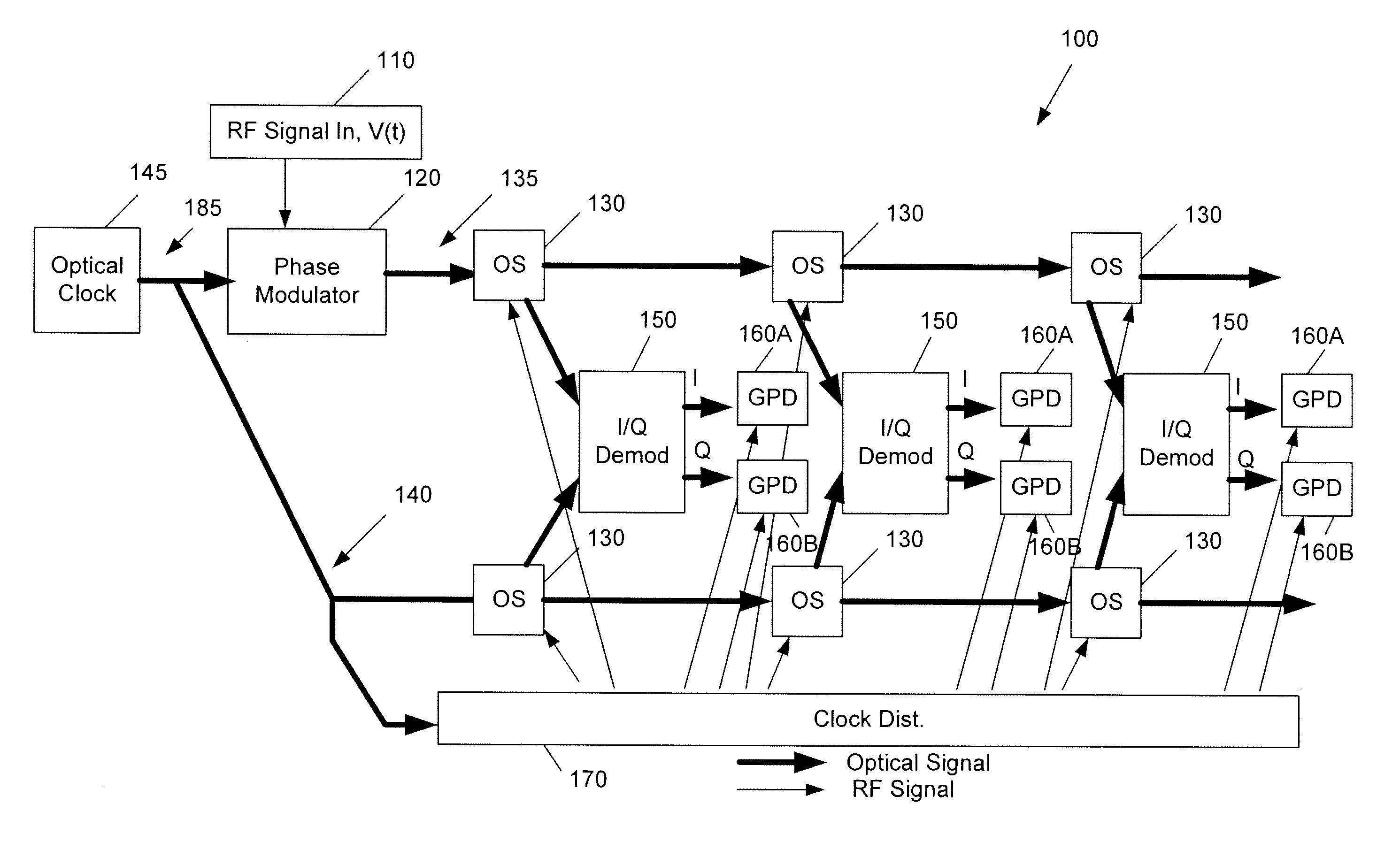
[0026]FIG. 1 shows a pADC 100 according to a The pADC 100 includes an optical clock 145 for the purpose of supplying a high repetition rate stream of optical pulses with very low clock jitter. Examples of this type of device include the mode locked laser (MLL) and coupled opto-electronic oscillator (COED).

[0027]The pADC 100 receives an rf voltage V(t) of an rf input signal 110. The rf input signal 110 can be received by a wide band antenna (not shown in FIG. 1), for example. The rf input signal 110 is input to a phase modulator 120, which performs phase modulation on the optical clock signal and which outputs a phase-modulated optical pulse stream.

[0028]The pADC 100 also includes a plurality of optical switches (OS) 130 connected in a series relationship to each other along a signal path 135. The plurality of optical switches 130 on the signal path 135 perform optical switching of the phase-modulated optical signal output by the phase modulator 120 in accordance with the series rel...

fourth embodiment

[0047]FIG. 6 shows an optical deserializer with gated detectors 700 in which the optical clock signal is amplitude modulated according to RF input signal 110 by amplitude modulator 710, The amplitude-modulated output of the amplitude modulator 710 is provided to n stages of optical switches 130 (n being an integer greater than one). The output of the last (nth) stage of optical switches 130 is provided to a plurality of pADCs 720, which perform analog-to-digital conversion of the optically-switched signals output by the last stage of optical switches 130. The digital outputs of the pADCs 720 are held by gated detectors 160A, 160B, . . . , to provide the “hold” function of a sample-and-hold circuit.

[0048]FIG. 7 is a block diagram of a clock distribution tree for the clock signals provided to components of a pADC or optical deserializer with gated detectors by the clock distribution unit according to the fourth exemplary embodiment. FIG. 7 also shows that the switching window shifts ...

fifth embodiment

[0049]FIG. 8 shows an optical deserializer with gated detectors 800 according to a The configuration of the optical deserializer with gated detectors 700 is similar to that as shown in FIGS. 1 and 3, but with the clock signal being amplitude modulated by amplitude modulator 710 according to the RF input signal 110 instead of being phase modulated by a phase modulator. Also, the processing of the rf input signal is shown as being performed by pADCs 720 instead of by I / Q Demodulators, whereby the pADCs provide digital outputs to gated detector 160A, 160B, . . . .


PUM


Abstract

A method of performing optical serial-to-parallel conversion of an optical signal includes performing phase modulation of the optical pulse stream and outputting a phase-modulated optical signal. Optical switching of the phase-modulated optical signal is performed by optical switches provided on a signal path. Optical switching of a reference optical clock signal is performed by optical switches provided on a reference path. I/Q demodulation of the optically switched phase-modulated optical signal respectively output by an optical switch is performed on the signal path at timings corresponding to the optically switched reference optical clock signal respectively output by an optical switch on the reference path, in which I and Q demodulated signals are output as a result thereof. Photodetection of the I and Q demodulated signals is then performed.

Description

FIELD OF THE INVENTION[0001]The present specification relates to optical deserialization with gated detectors. More particularly, the present specification relates to a photonic analog-to-digital converter (pADC) that performs optical deserialization with gated detectors for use in high frequency (e.g., 100+ MHz and multi-GHz) radio frequency (rf) systems.[0002]Optical system designers have utilized optical deserialization as a component of pADCs used in high frequency (e.g., 100+ MHz and multi-GHz) systems. Fundamental performance limits of conventional pADCs significantly constrain the potential of these devices, such as systems operating wide band in excess of several GHz.[0003]Therefore, there is a need to have a pADC that performs optical deserialization with gated detectors and that has increased resolution compared to a conventional pADC that performs optical deserialization.SUMMARY OF THE INVENTION[0004]An exemplary embodiment relates to a photonic Analog-to-Digital Converte...

Claims


Application Information

Patent Timeline
IPC IPC(8): H03M1/12
CPCG02F7/00H03M1/1245G02F2203/50H03M1/1215
Inventor ZANONI, RAYMONDJEPSEN, KIM S.LALIBERTE, MARK A.KING, OLIVER S.
Owner ROCKWELL COLLINS INC
Why Eureka
Try Eureka