
Flux-quantizing superconducting analog to digital converter (ADC)

a superconducting analog to digital converter and flux-quantization technology, applied in analogue/digital conversion, transmission systems, instruments, etc., can solve the problems of significant constraints on the maximum speed of response and limitation of the dynamic range of input signals, and achieve the effect of increasing the dynamic range of quantizers

Inactive Publication Date: 2008-02-28
HYPRES
View PDF4 Cites 18 Cited by
  • Summary
  • Abstract
  • Description
  • Claims
  • Application Information

AI Technical Summary

Benefits of technology

[0010]Consequently for a given voltage amplitude at the input node which would tend to cause a JJ to switch at a frequency of f1, the components in the first and second branch only have to switch at a frequency of f1 / 2 with the alternating output signals at the first and second outputs having a frequency of f1 / 2 . This enables either higher frequency operation or a more relaxed design of the components within the loop.
[0012]A bias voltage generating circuit embodying the invention may include a high frequency superconducting clock and a flux pump which includes one or more phase generators including confluence buffers for generating a bias voltage which can, in turn, cause the generation of pulse signals which have a higher frequency than the high frequency superconducting clock signal. In one embodiment, the outputs of the flux pump are supplied to an inductive merging circuit for generating a bias voltage (also referred to as an offset or pedestal), which adds to the bipolar analog input signal, generating a combined analog signal which is unipolar. Since this voltage offset is generated from the clock signal, it can be accurately subtracted off digitally at a later time.

Problems solved by technology

This imposes significant constraints on the maximum speed of response at which the circuit can provide a linear response.
There thus exits a limitation on the dynamic range of the input signal which can be processed linearly by the single junction quantizer.

Method used


Image

  • Flux-quantizing superconducting analog to digital converter (ADC)
  • Flux-quantizing superconducting analog to digital converter (ADC)
  • Flux-quantizing superconducting analog to digital converter (ADC)

Examples


Embodiment Construction

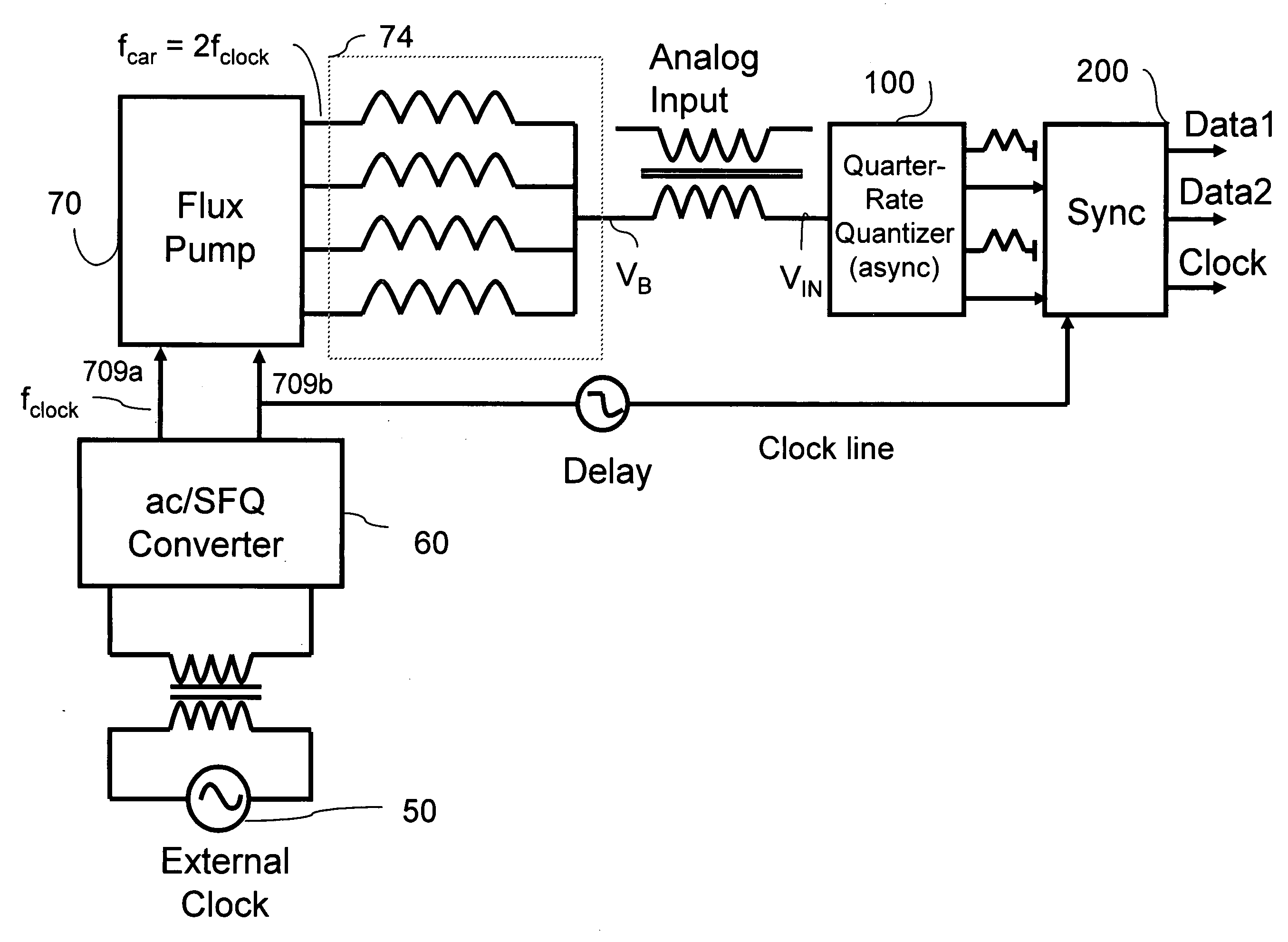
[0029]FIG. 2 is a block diagram of an ADC system embodying the invention. The system of FIG. 2 includes circuitry for performing the analog to digital conversion and circuitry for generating a bias (offset) voltage for the analog signal applied to the conversion circuit. The bias voltage generator includes an external clock circuit 50 coupled via an ac / SFQ converter circuit 60 to a flux pump 70 whose outputs are merged via an inductive network 74 to generate a bias voltage (VB) which is superimposed on the analog input signal to generate an analog input signal Vin which is applied to a quarter-rate (divide by four) quantizer 100. The quantizer 100 converts the amplitude of an analog voltage (Vin) into pulse streams which can be digitally processed via circuitry which can be synchronized to the basic clock circuit.

[0030]The bias generating circuitry shown in FIG. 2 may be implemented as shown in FIGS. 3, and 3A though 3D. In FIG. 3, the flux pump 70 is formed using four (4) phase gen...


PUM


Abstract

A superconducting analog-to-digital converter includes a superconducting input loop to which is applied an analog voltage to be converted to a digital format. The superconducting loop includes two Josephson junctions for converting said analog input voltage into a single flux quantum (SFQ) pulse stream having a frequency f1 which is directly proportional to the amplitude of the analog input voltage. The loop includes two outputs for distributing the pulse stream in a cyclical and staggered fashion onto the two loop outputs such that the frequency of the pulses along each one of the loop outputs is f1 / 2. Additional frequency divider circuits may be coupled to the loop outputs to produce pulse streams on N output lines having a frequency of f1 / N.

Description

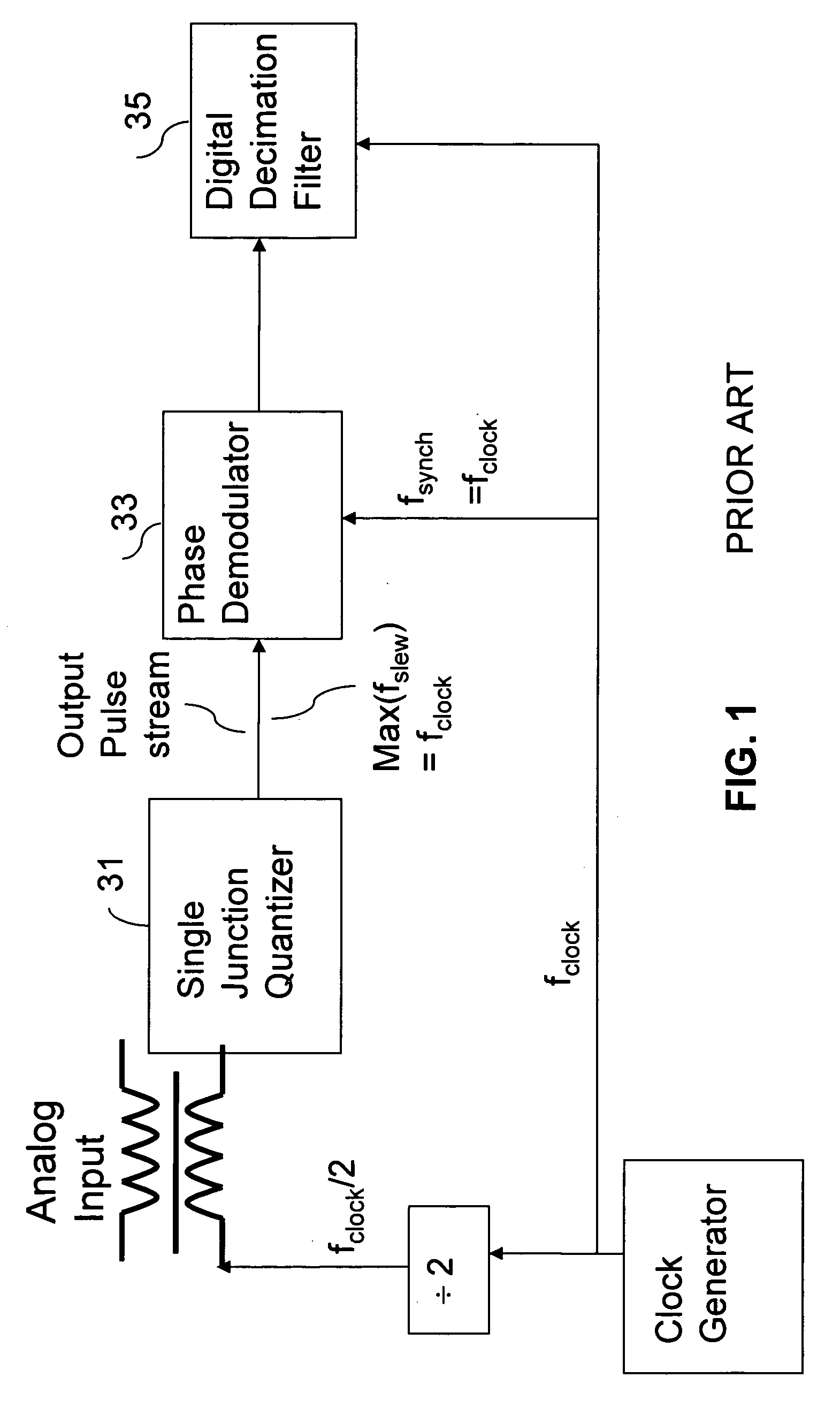
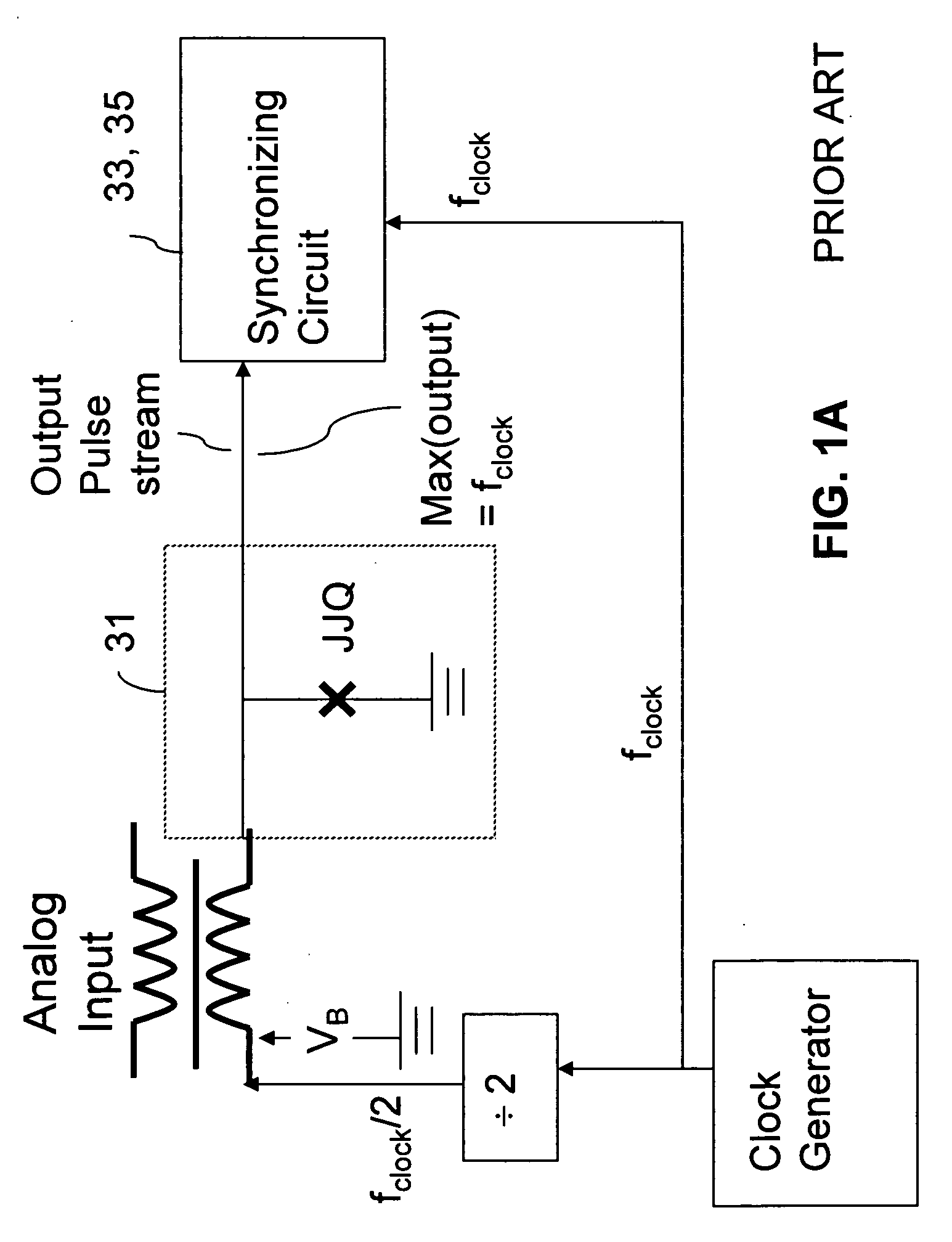
BACKGROUND TO THE INVENTION[0001]This invention relates to superconducting integrated circuits and, in particular, to high speed superconducting analog-to-digital converters (ADCs).[0002]Important measures of the performance of an ADC include speed, i.e., the sampling rate in samples converted per second, resolution or sensitivity as measured by the smallest change that can be measured in an analog signal and dynamic range. Ultrafast superconducting digital circuits may be fabricated using Josephson junctions (JJs) integrated together according to RSFQ (rapid-single-flux-quantum) Logic. Furthermore, JJs are well suited to form a natural high-resolution ADC, since a voltage V applied across a JJ (with appropriate damping) generates a rapid sequence of single-flux-quantum (SFQ) digital pulses at a rate determined by fundamental constants defined by f=2 eV / h, where: f is frequency, V is the voltage applied across the JJ, “e” is the charge on an electron, and “h” is Planck's constant. C...

Claims


Application Information

Patent Timeline
Patent Type & Authority Applications(United States)
IPC IPC(8): H03M1/12
CPCH03M1/60H03M1/1215
Inventor RYLOV, SERGEYINAMDAR, AMOL
Owner HYPRES
Learn More