Semiconductor device and manufacturing method thereof

a technology of semiconductors and semiconductors, applied in semiconductor devices, electrical devices, transistors, etc., can solve the problems of reducing yield and no option but to sacrifice the electric characteristics of transistors, and achieve the effects of reducing the number of photolithography steps, high display quality, and reducing the parasitic capacitance in the intersection portion

Active Publication Date: 2013-06-11
SEMICON ENERGY LAB CO LTD
View PDF134 Cites 14 Cited by
  • Summary
  • Abstract
  • Description
  • Claims
  • Application Information

AI Technical Summary

Benefits of technology

[0012]An object is to reduce the number of photolithography steps in a manufacturing process of a semiconductor device. Further, an object is to manufacture a display device having high display quality.
[0018]The capacitor portion includes a capacitor wiring formed using the same material and in the same layer as the gate electrode, which also serves as a common wiring; an insulating film formed using the same material and in the same layer as the gate insulating film, which serves as a dielectric film; and a capacitor electrode formed using the same material and in the same layer as the transparent conductive film. Here, the dielectric film may include a semiconductor film formed using the same material and in the same layer as the semiconductor film and an insulating film formed using the same material and in the same layer as the channel protective film. Note that the number of layers included in the dielectric film is preferably smaller because the area occupied by the capacitor portion can be reduced when the dielectric film is made thinner, and the aperture ratio of the display device can be increased.
[0022]Note that in an intersection portion of the common wiring and the source wiring, the insulating film formed using the same material and in the same layer as the gate insulating film, the semiconductor film formed using the same material and in the same layer as the semiconductor film, and the insulating film formed using the same material and in the same layer as the channel protective film are preferably provided between the common wiring and the source wiring. With such a structure, parasitic capacitance in the intersection portion can be reduced. Thus, a display device in which the number of photolithography steps is reduced and display quality is high can be provided.
[0024]As compared to a conventional display device, the number of photolithography steps can be reduced, so that an increase in cost can be suppressed even when a larger substrate is used.

Problems solved by technology

Using such complicated techniques might cause various problems, thereby leading to reduction in yield.
Moreover, there has often been no option but to sacrifice electric characteristics of transistors.

Method used


Image

  • Semiconductor device and manufacturing method thereof
  • Semiconductor device and manufacturing method thereof
  • Semiconductor device and manufacturing method thereof

Examples


embodiment 1

(Embodiment 1)

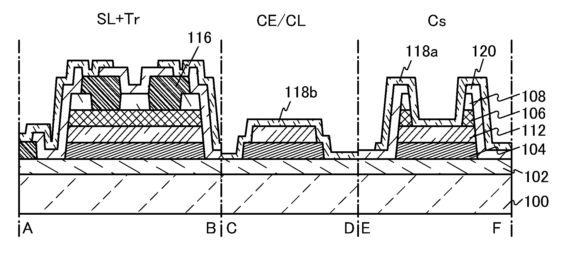
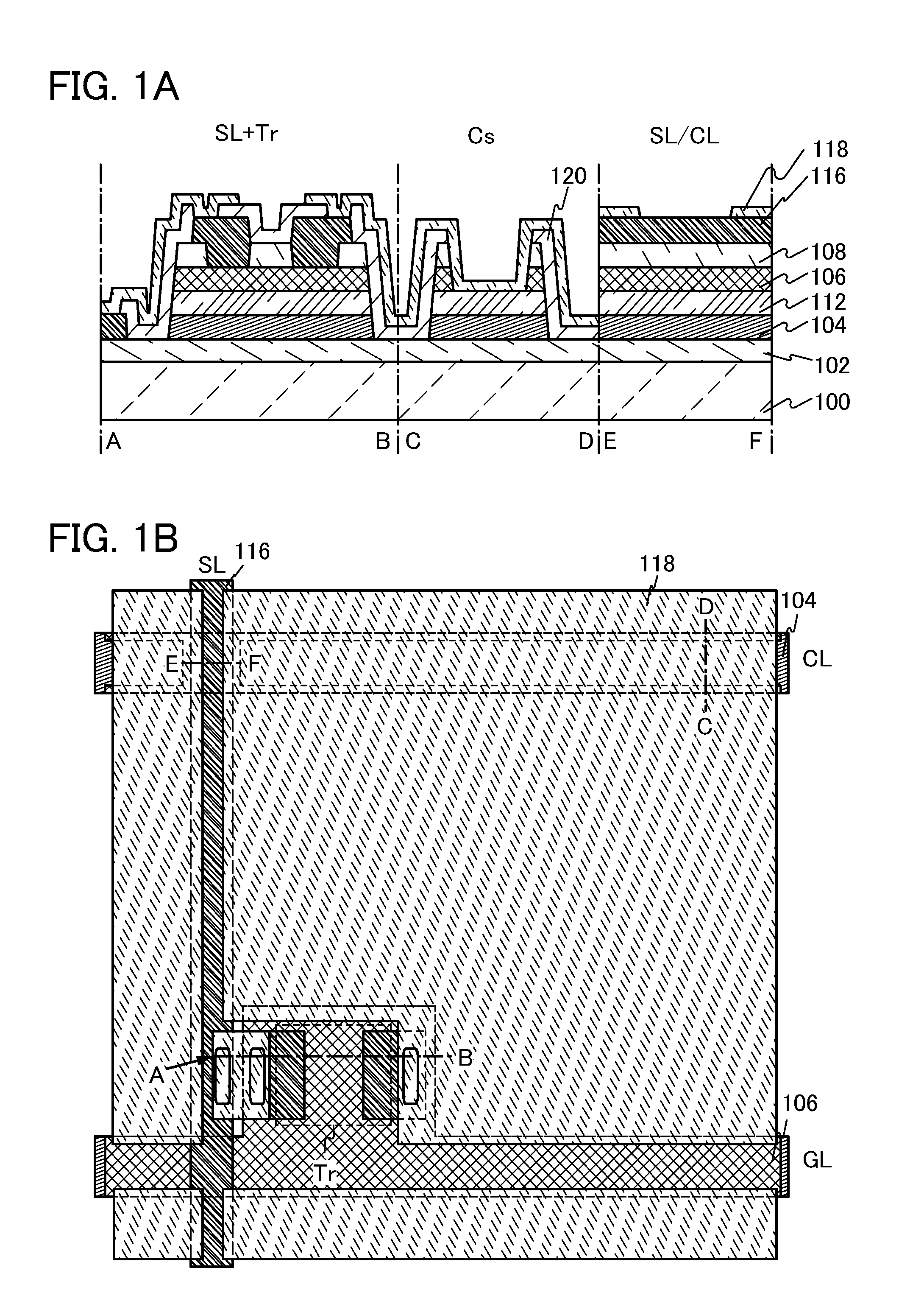
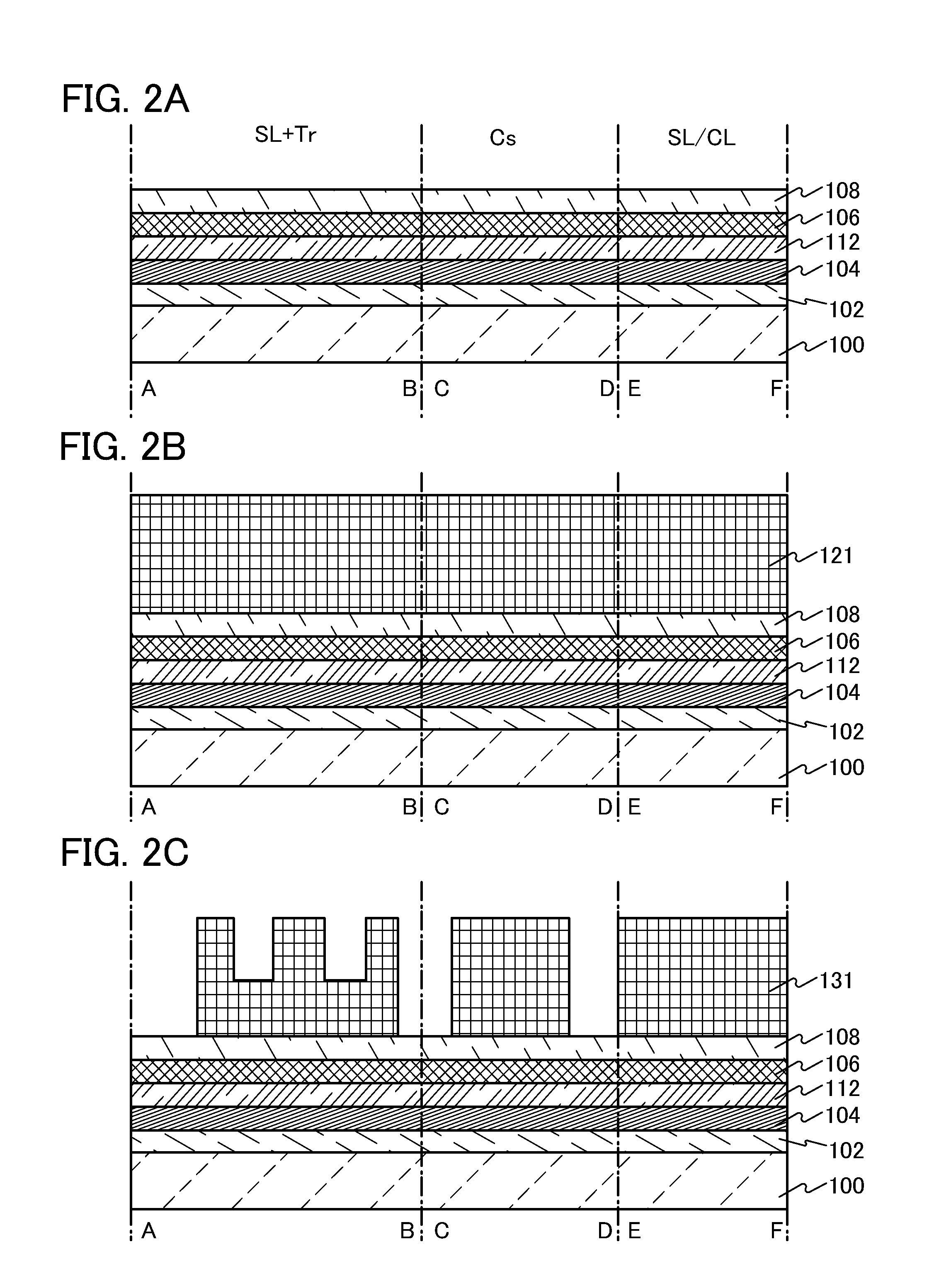
[0046]First, a semiconductor device (a transistor and a capacitor portion of a display device) which is one embodiment of the present invention will be described with reference to FIGS. 1A and 1B, FIGS. 2A to 2C, FIGS. 3A to 3C, FIGS. 4A to 4C, FIGS. 5A to 5C, FIGS. 6A to 6C, FIGS. 7A to 7C, FIGS. 10A and 10B, and FIGS. 17A and 17B. A source wiring SL and a transistor Tr, a capacitor portion Cs, and an intersection portion of the source wiring SL and a common wiring CL (also serving as a capacitor wiring) will be described in parallel with reference to FIGS. 1A and 1B, FIGS. 2A to 2C, FIGS. 3A to 3C, FIGS. 4A to 4C, FIGS. 5A to 5C, FIGS. 6A to 6C, FIGS. 7A to 7C, FIGS. 10A and 10B, and FIGS. 17A and 17B.

[0047]FIGS. 1A and 1B are a cross-sectional view and a top view of a semiconductor device manufactured in this embodiment. FIG. 1A illustrates cross sections A-B, C-D, and E-F along dashed lines A-B, C-D, and E-F in FIG. 1B. Note that some films are omitted in FIG. 1B f...

embodiment 2

(Embodiment 2)

[0108]In this embodiment, a semiconductor device (a transistor and a capacitor portion of a display device) having a structure different from that described in Embodiment 1 will be described with reference to FIGS. 11A and 11B, FIGS. 12A and 12B, FIGS. 13A and 13B, and FIGS. 14A to 14C. The source wiring SL and the transistor Tr, a connection portion of a common electrode CE and the common wiring CL, and the capacitor portion Cs will be described in parallel with reference to FIGS. 11A and 11B, FIGS. 12A and 12B, FIGS. 13A and 13B, and FIGS. 14A to 14C.

[0109]In this embodiment, a semiconductor device which can be applied to a liquid crystal display device of an in-plane switching (IPS) mode which is a kind of horizontal electric field modes will be described.

[0110]FIGS. 11A and 11B are a cross-sectional view and a top view of a display device manufactured in this embodiment. FIG. 11A illustrates cross sections A-B, C-D, and E-F along dashed lines A-B, C-D, and E-F in F...

embodiment 3

(Embodiment 3)

[0133]In this embodiment, a semiconductor device (a transistor and a capacitor portion of a display device) having a structure different from those in Embodiment 1 and Embodiment 2 will be described with reference to FIGS. 15A and 15B and FIGS. 16A to 16C. The source wiring SL and the transistor Tr, the connection portion of the common electrode CE and the common wiring CL, and a region where the common electrode CE and a pixel electrode TE overlap with each other will be described in parallel with reference to FIGS. 15A and 15B and FIGS. 16A to 16C.

[0134]In this embodiment, a semiconductor device which can be applied to a liquid crystal display device of a fringe field switching (FFS) mode which is a kind of horizontal electric field modes will be described.

[0135]Since a region where the common electrode CE and the pixel electrode TE overlap with each other forms a capacitor portion in a liquid crystal display device of an FFS mode, it is not needed to form a capacito...


PUM


Abstract

A conductive film to be a gate electrode, a first insulating film to be a gate insulating film, a semiconductor film in which a channel region is formed, and a second insulating film to be a channel protective film are successively formed. With the use of a resist mask formed by performing light exposure with the use of a photomask which is a multi-tone mask and development, i) in a region without the resist mask, the second insulating film, the semiconductor film, the first insulating film, and the conductive film are successively etched, ii) the resist mask is made to recede by ashing or the like and only the region of the resist mask with small thickness is removed, so that part of the second insulating film is exposed, and iii) the exposed part of the second insulating film is etched, so that a pair of opening portions is formed.

Description

BACKGROUND OF THE INVENTION[0001]1. Field of the Invention[0002]The present invention relates to a semiconductor device and a manufacturing method thereof.[0003]In this specification, a semiconductor device means all types of devices that can function by utilizing semiconductor characteristics, and a semiconductor circuit, a memory device, an imaging device, a display device, an electro-optical device, an electronic device, and the like are all semiconductor devices.[0004]2. Description of the Related Art[0005]In recent years, transistors that are formed using a semiconductor thin film having a thickness of several nanometers to several hundreds of nanometers over a substrate having an insulating surface such as a glass substrate have been attracting attentions. Transistors are widely used for electronic devices such as integrated circuits (ICs) and electro-optical devices. In particular, transistors are urgently developed as switching elements of display devices typified by liquid ...

Claims


Application Information

Patent Timeline
Patent Type & Authority Patents(United States)
IPC IPC(8): H01L29/66
CPCH01L27/1288H01L27/1225
Inventor ENDO, YUTANODA, KOSEI
Owner SEMICON ENERGY LAB CO LTD
Why Eureka
Try Eureka