Semiconductor integrated circuit device, design method, design apparatus, and program

a technology of integrated circuit devices and semiconductors, applied in semiconductor/solid-state device details, semiconductor/solid-state device devices, instruments, etc., can solve the problems affecting the performance of transistors, and reducing the area of semiconductor integrated circuit devices. , to achieve the effect of reducing the area of semiconductor integrated circuit devices

Inactive Publication Date: 2013-07-09
RENESAS ELECTRONICS CORP
View PDF15 Cites 8 Cited by
  • Summary
  • Abstract
  • Description
  • Claims
  • Application Information

AI Technical Summary

Benefits of technology

[0012]In the semiconductor integrated circuit device having a configuration as described above, the wires coupled to the respective one comparison input terminals have one terminals thereof coupled to the transistor gates and the other terminals thereof coupled to the diffusion layer serving as the ladder resistor LDR. As a result, the antenna effect of the wiring that occurs during manufacturing is reduced by the diffusion layer serving as the ladder resistor LDR.
[0014]In the semiconductor integrated circuit device having a configuration as described above, the metal wire M1 has one terminal thereof coupled to the gate of the NMOS transistor MN2, another terminal thereof coupled to the diffusion layer DF, and still another terminal thereof coupled to the drain (diffusion layer) of the NMOS transistor MN1. As a result, the antenna effect of the metal wire M1 that occurs during manufacturing is reduced by the diffusion layer DF and the drain of the NMOS transistor MN1.
[0015]On the other hand, the metal wire M2 has one terminal thereof coupled to the gate of the NMOS transistor MN3, and the other terminal thereof coupled to the diffusion layer DF. As a result, the antenna effect of the metal wire M2 that occurs during manufacturing is reduced by the diffusion layer DF.
[0022]According to the present invention, layout of the semiconductor integrated circuit device is performed so as to satisfy the design standard associated with the antenna ratio that has been moderated using the diffusion layer region, and the area of the semiconductor integrated circuit device can be reduced.

Problems solved by technology

If the accumulated charges exceed a given amount, the breakdown or degradation of a gate oxide film is caused thereby, or the performance of a transistor is degraded thereby.
As a semiconductor device process has been increasingly miniaturized, the influence of not only the area of wiring but also a layout in the vicinity of the wiring increases to make it difficult to obtain a semiconductor integrated circuit which is sufficiently stable against the antenna effect.
As a result, the area of wiring directly coupled to the gate is limited more than necessary.
In the prior art technology, even when consideration is given to a variation component based on the effect of reducing the antenna effect, it is not disclosed how the consideration should be given with regard to a semiconductor integrated circuit device having an exemplary configuration as described above in which two or more independent metal wires are coupled to one of diffusion layers, and proper design cannot be performed.
As a result, design with sufficient allowance should be performed, and the area of the semiconductor integrated circuit device cannot be reduced for a circuit as a design target.

Method used


Image

  • Semiconductor integrated circuit device, design method, design apparatus, and program
  • Semiconductor integrated circuit device, design method, design apparatus, and program
  • Semiconductor integrated circuit device, design method, design apparatus, and program

Examples


first embodiment

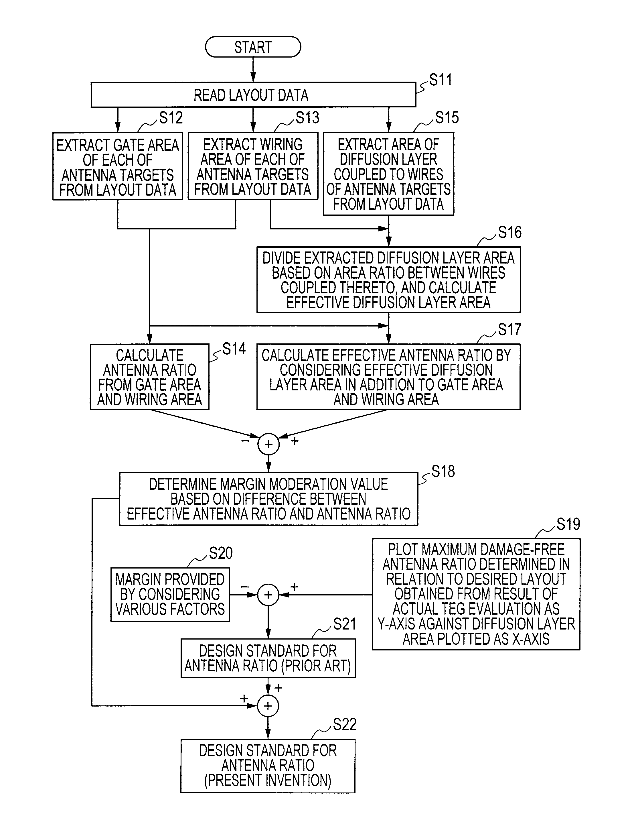
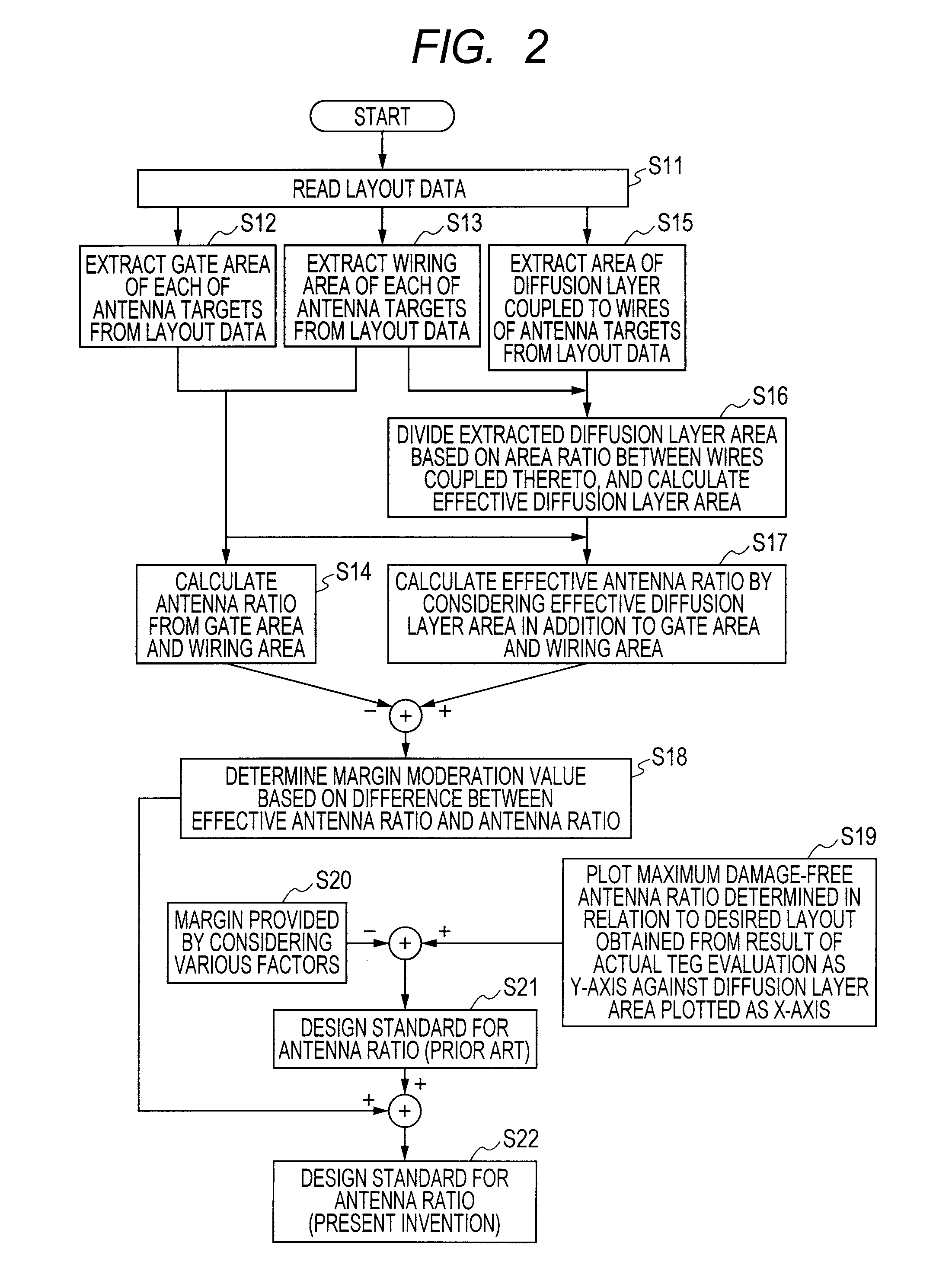
[0040]FIG. 1 is a view showing a configuration of a design apparatus according to a first embodiment of the present invention. In FIG. 1, the design apparatus includes a layout data accumulation section 11, an antenna ratio calculation section 12, and a layout verification section 13. The layout data accumulation section 11 holds in advance layout data of a semiconductor integrated circuit device as a design target, and further holds layout data as the result of verification performed in the layout verification section 13. The antenna ratio calculation section 12 reads the layout data from the layout data accumulation section 11, extracts components from which two or more independent metal wires are coupled to one of diffusion layer regions based on the layout data, determines, for each of the components, the area of each of the two or more independent metal wires and the area of each of electrodes coupled to the respective metal wires, determines an antenna ratio between the area o...

second embodiment

[0071]A semiconductor integrated circuit device of the second embodiment is the semiconductor integrated circuit device for verification which includes the test element group (TEG) for the evaluation of a process characteristic. Each of test elements is configured such that two or more independent metal wires are coupled to one of diffusion layer regions, and a gate electrode is coupled to each of the metal wires.

[0072]FIG. 7 is a view showing an example of a configuration of the test element group mounted in the semiconductor integrated circuit device according to the second embodiment. For example, in the test element corresponding to the uppermost row in FIG. 7, independent N (N is an integer of not less than 2) metal wires (antenna nodes) are coupled to a diffusion layer region having an area of 0.1 μm2, and a gate electrode having an area of 0.1 μm2 is coupled to each of the metal wires. The area of each of the N metal wires is 10*ai μm2. Here,

[0073]ai=i / ∑i=1N⁢i

is satisfied. Fo...


PUM


Abstract

An antenna ratio calculation section extracts components from which two or more independent metal wires are coupled to one of diffusion layer regions based on layout data read from a layout data accumulation section, determines, for each of the components, the area of each of the two or more independent metal wires and electrodes coupled to the respective metal wires, determines an antenna ratio between the area of each of the metal wires and the area of the electrode coupled to the metal wire, and determines a moderation value for moderating a design standard associated with plasma charge damage related to one of the metal wires based on the ratio of the total area of all the metal wires coupled to the one of the diffusion layer regions to the area of the one of the metal wires.

Description

CROSS-REFERENCE TO RELATED APPLICATIONS[0001]The disclosure of Japanese Patent Application No. 2010-38973 filed on Feb. 24, 2010 including the specification, drawings and abstract is incorporated herein by reference in its entirety.BACKGROUND[0002]1. Field of the Invention[0003]The present invention relates to a semiconductor integrated circuit device, a design method, a design apparatus, and a program, and particularly to a technology for designing a semiconductor integrated circuit device so as to prevent breakdown or degradation due to a charge-up phenomenon in manufacturing steps thereof.[0004]2. Description of the Related Art[0005]In manufacturing steps of a semiconductor integrated circuit, a plasma or ion beam technique is used. In such steps, when wiring of the semiconductor integrated circuit is coupled to a gate electrode, charges are accumulated in the wiring. If the accumulated charges exceed a given amount, the breakdown or degradation of a gate oxide film is caused the...

Claims


Application Information

Patent Timeline
Patent Type & Authority Patents(United States)
IPC IPC(8): G06F17/50H01L23/50
CPCG06F17/5063H01L23/66G06F2217/12H01L23/535H01L2924/0002H01L2223/6677H01L2924/00G06F30/36G06F2119/18Y02P90/02
Inventor SAKAMOTO, HIDEO
Owner RENESAS ELECTRONICS CORP
Why Eureka
Try Eureka