Light-emitting element, light-emitting device, electronic device, and lighting device

a technology of light-emitting elements and light-emitting layers, which is applied in the direction of organic semiconductor devices, discharge tubes luminescnet screens, natural mineral layered products, etc., can solve the problems of difficult substantial removal of elements, inability to realize the work function of anodes, and inability to meet the homo level of light-emitting layers, etc., to achieve excellent emission efficiency and drive voltage, long life, and long life

Active Publication Date: 2013-07-16
SEMICON ENERGY LAB CO LTD
View PDF114 Cites 14 Cited by
  • Summary
  • Abstract
  • Description
  • Claims
  • Application Information

AI Technical Summary

Benefits of technology

[0099]In this specification, the HOMO levels that are substantially equalized mean, specifically, HOMO levels that differ from each other by greater than or equal to −0.2 eV and less than or equal to +0.2 eV. This is because electrochemical reaction energies differing by 0.2 eV or less can be regarded as roughly the same electrochemical reaction energy; usually, in the case where the electrochemical reaction energy difference between two kinds of substances is 0.2 eV or less, both two types of electrochemical reactions occur (on the other hand, if the difference greatly exceeds 0.2 eV, only one type of electrochemical reaction occurs selectively). The experiment described later in Example also shows that an effect of the invention can be obtained with a HOMO level difference greater than or equal to −0.2 eV and less than or equal to +0.2 eV. A HOMO level difference greater than or equal to −0.1 eV and less than or equal to +0.1 eV is further preferable to achieve an effect of the invention to a higher extent.
[0100]With the increasing energy gap of the third organic compound in the light-emitting layer 121, the HOMO level 135 of the third organic compound tends to decrease. Therefore, when the above structure reduces the hole-injection barriers between the first layer 111 and the second layer 112 and between the second layer 112 and the light-emitting layer 121, all the HOMO levels of the first, second, and third organic compounds become significantly lower than the work function 131 of the anode. Accordingly, a large hole-injection barrier is formed between the work function 131 of the anode and the HOMO level 133 of the first organic compound, which hampers hole injection from the anode 101 to the first layer 111.
[0101]Accordingly, as a solution to this barrier at the anode interface, the present inventors have considered adding the electron-accepting compound to the first layer 111. By the addition of the electron-accepting compound to the first layer 111, holes are injected smoothly even when there is a gap between the work function 131 of the anode and the HOMO level 133 of the first organic compound included in the first layer 111; thus, the hole-injection barrier is substantially removed. As the first layer 111, the electron-accepting compound and the first organic compound may be combined, or may be layered in order from the anode.
[0102]The above-described structure substantially removes hole-injection barriers between the layers from the anode to the light-emitting layer which have been problematic in a conventional element. However, it has been found that merely adopting such a structure causes holes to easily pass to the cathode, leading to lower emission efficiency. It has been also found that the structure causes an electron-transport layer to emit light in the case where it is provided between the light-emitting layer 121 and the cathode 102.
[0103]In order to prevent holes from passing to the cathode without using a barrier (a block to holes), adding a substance having a hole-trapping property is effective. The present inventors have thoroughly examined the kinds of the substance having a hole-trapping property and a region where the substance is to be added. The inventors have accordingly found that, by making a light-emitting substance added to a light-emitting layer have a hole-trapping property, the above problem can be solved without increasing drive voltage. In order that holes be trapped by the light-emitting substance, the third organic compound and the light-emitting substance having a hole-trapping property are preferably a host material and a guest material, respectively. Further, a HOMO level 136 of the light-emitting substance having a hole-trapping property is preferably higher than the HOMO level 135 of the third organic compound by 0.3 eV or more in view of the above-described electrochemical selectivity.
[0104]Merely preventing holes from passing to the cathode for higher emission efficiency can be achieved also by adding a material for trapping holes between the anode 101 and the light-emitting layer 121. However, such a technique reduces the speed of hole transport until holes reach the light-emitting layer 121 to emit light, thereby inevitably increasing drive voltage. Further, a carrier recombination region might approach the anode to cause electrons to pass to the anode, thereby lowering emission efficiency. In contrast, in the structure of one embodiment of the present invention illustrated in FIGS. 1A and 1B, holes are transported from the anode 101 to the light-emitting layer 121 without influence of a barrier or a trap, and accordingly the drive voltage increase can be minimized. In short, it is preferable that a material having a hole-trapping property be not added to the second layer.

Problems solved by technology

However, the above design causes difficulty with an increasing difference between the work function of an anode and the HOMO level of a light-emitting layer.
Such an element is not practical.
Therefore, a hole-injection barrier between a hole-injection layer and a hole-transport layer or between a hole-transport layer and a light-emitting layer is able to be reduced but difficult to substantially remove.
This increases the difference between the work function of the anode and the HOMO level of the light-emitting layer, causing a large hole-injection barrier.
In many cases, the hole-injection barrier between a hole-transport layer and a light-emitting layer tends to be large.

Method used


Image

  • Light-emitting element, light-emitting device, electronic device, and lighting device
  • Light-emitting element, light-emitting device, electronic device, and lighting device
  • Light-emitting element, light-emitting device, electronic device, and lighting device

Examples


embodiment 1

[0091]Embodiment 1 will provide descriptions of a structure of a light-emitting element which is one embodiment of the present invention referring to a material to be used and a fabrication method. In Embodiment 1, a region interposed between an anode and a cathode is called an EL layer.

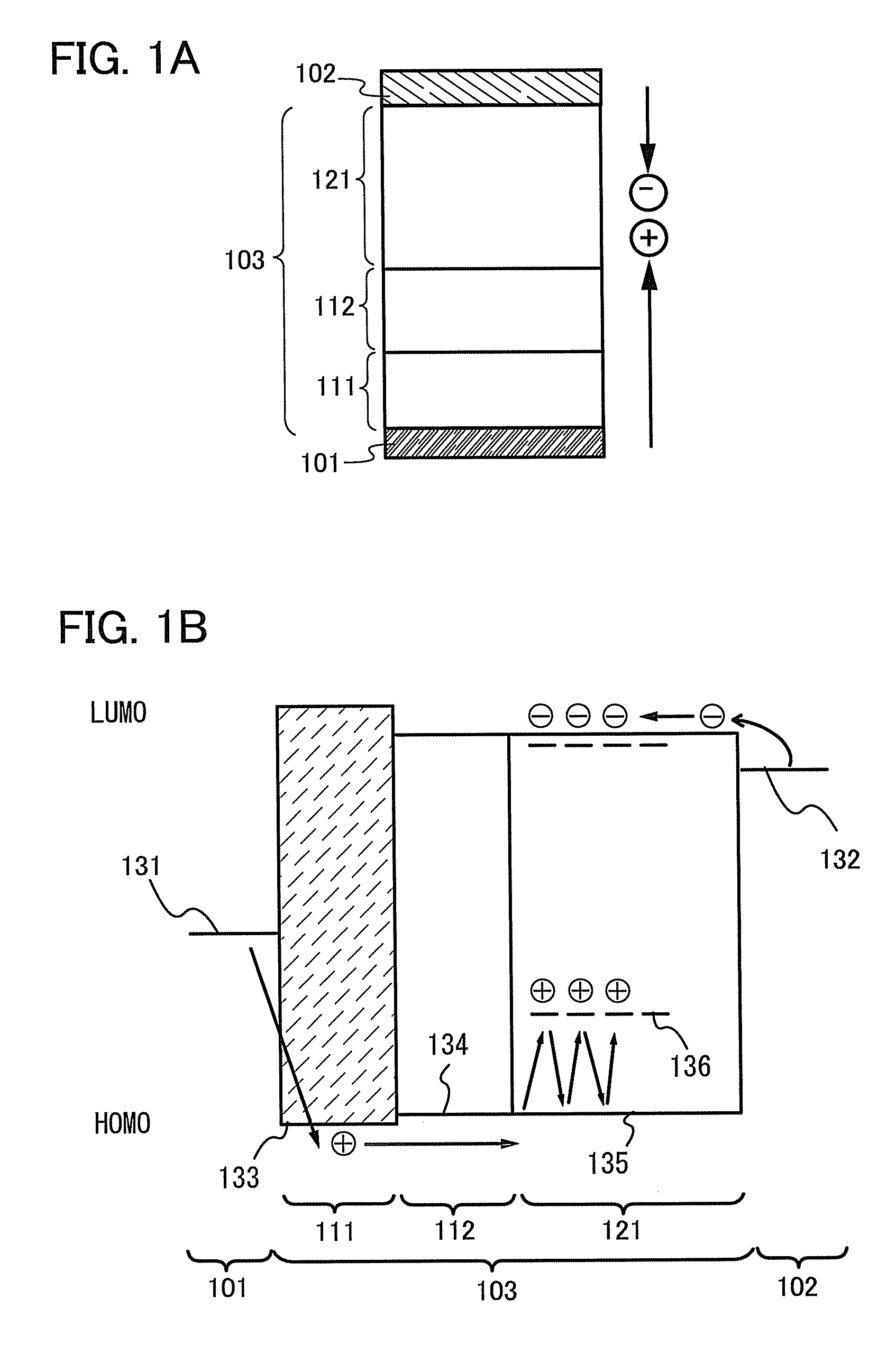
[0092]First, FIGS. 1A and 1B illustrate respectively a conceptual element structure and its band diagram of the light-emitting element of one embodiment of the present invention. For comparison, FIGS. 2A and 2B illustrate respectively a conceptual element structure and its band diagram of a conventional light-emitting element.

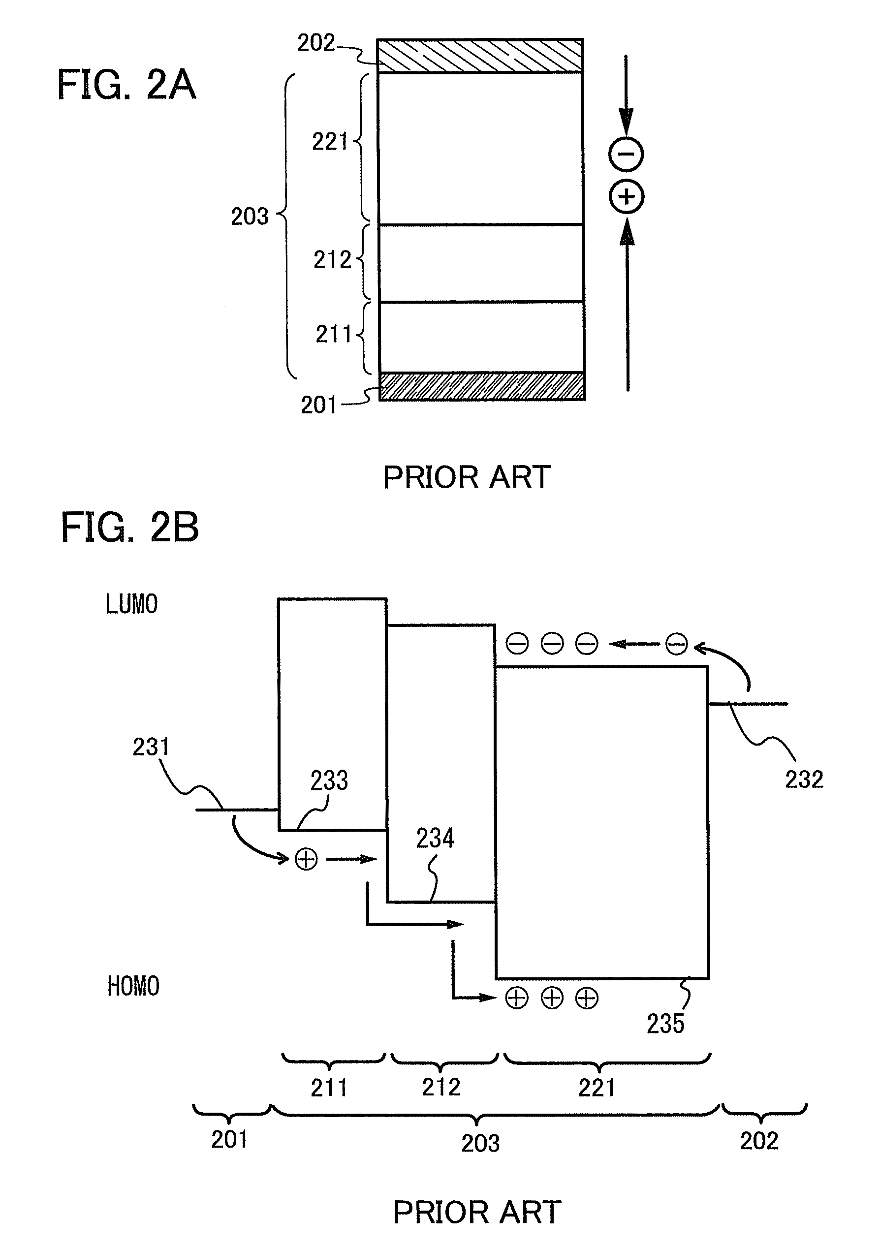
[0093]FIG. 2A illustrates the element structure of the conventional light-emitting element as described in, for instance, Non-Patent Document 3, which has an EL layer 203 provided between an anode 201 and a cathode 202. The EL layer 203 has a stack structure where a hole-injection layer 211, a hole-transport layer 212, and a light-emitting layer 221 are provided in order from th...

embodiment 2

[0160]Embodiment 2 will provide descriptions of a structure preferred for higher carrier recombination efficiency of the light-emitting element which is one embodiment of the present invention, referring to a material to be used and a fabrication method. In Embodiment 2, a region interposed between an anode and a cathode is called an EL layer.

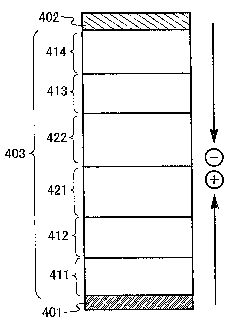
[0161]FIGS. 4A and 4B illustrate respectively a conceptual element structure and its band diagram of the light-emitting element of one embodiment of the present invention in Embodiment 2. As illustrated in FIG. 4A, in a light-emitting element of one embodiment of the present invention, an EL layer 403 is provided between an anode 401 and a cathode 402. The EL layer 403 at least has a stack structure where a first layer 411, a second layer 412, a first light-emitting layer 421, and a second light-emitting layer 422 are provided in order from the anode 401. Further, the first layer 411 contains the first organic compound and the electron-acceptin...

embodiment 3

[0217]This embodiment will provide descriptions of a structure of the light-emitting layer, which is different from those in Embodiments 1 and 2. Note that a structure of a light-emitting element will be described using FIGS. 1A and 1B.

[0218]In FIGS. 1A and 1B, although the light-emitting layer 121 includes the third organic compound and the light-emitting substance having a hole-trapping property with respect to the third organic compound according to Embodiment 1, the light-emitting layer 121 includes a light-emitting substance capable of emitting light (a substance having a light-emitting property) which is different from the light-emitting substance having a hole-trapping property according to Embodiment 3. That is, the light-emitting layer 121 of this embodiment includes the substance having a light-emitting property in addition to the light-emitting substance having a hole-trapping property.

[0219]Since the structure in FIGS. 1A and 1B according to Embodiment 3, which is except...


PUM

PropertyMeasurementUnit
HOMOaaaaaaaaaa
LUMOaaaaaaaaaa
HOMO levelaaaaaaaaaa

Abstract

Objects of the present invention are to provide: a light-emitting element having a long lifetime and good emission efficiency and drive voltage. One embodiment of the invention is a light-emitting element including, between an anode and a cathode, at least a stack structure in which a first layer, a second layer, and a light-emitting layer are provided in order from the anode side. The first layer includes a first organic compound and an electron-accepting compound. The second layer includes a second organic compound having a HOMO level differing from the HOMO level of the first organic compound by from −0.2 eV to +0.2 eV. The light-emitting layer includes a third organic compound having a HOMO level differing from the HOMO level of the second organic compound by from −0.2 eV to +0.2 eV and a light-emitting substance having a hole-trapping property with respect to the third organic compound.

Description

BACKGROUND OF THE INVENTION[0001]1. Field of the Invention[0002]The present invention relates to a light-emitting element, a light-emitting device, an electronic device, and a lighting device.[0003]2. Description of the Related Art[0004]In recent years, research and development have been extensively conducted on light-emitting elements using electroluminescence (EL). In the basic structure of such a light-emitting element, a layer which contains a substance having a light-emitting property is interposed between a pair of electrodes. By voltage application to this element, the substance having a light-emitting property can emit light.[0005]Since such light-emitting elements are self-luminous elements, they have advantages over liquid crystal displays in having high visibility of pixels and eliminating the need for a backlight, for example, thereby being considered as suitable for flat panel display elements. Also, above-described light-emitting elements have an advantage in that they...

Claims


Application Information

Patent Timeline
Patent Type & Authority Patents(United States)
IPC IPC(8): H01L51/54
CPCH01L51/0052H01L51/0054H01L51/0072H01L51/0073H01L51/0071H01L51/0085H01L51/0074H01L2251/552H01L51/5036H01L51/5048H01L51/5088H10K50/11H10K2101/40H10K50/15H10K50/17H10K85/622H10K85/615H10K85/6576H10K85/6574H10K85/6572H10K85/342H10K50/125H10K50/14H10K2101/30H10K85/657C09K11/06H10K85/324H10K85/626H10K85/633H10K85/6565
Inventor SEO, SATOSHISUZUKI, TSUNENORISHITAGAKI, SATOKO
Owner SEMICON ENERGY LAB CO LTD
Why Eureka
Try Eureka