Offset cancelling circuit

a technology of offset cancelling circuit and output voltage, which is applied in the direction of galvano-magnetic hall-effect devices, instruments, pulse techniques, etc., can solve the problem that the offset value of the output voltage of the hall element cannot be accurately cancelled

Active Publication Date: 2013-08-06
SEMICON COMPONENTS IND LLC
View PDF12 Cites 0 Cited by
  • Summary
  • Abstract
  • Description
  • Claims
  • Application Information

AI Technical Summary

Problems solved by technology

However, in a normal Hall element, there is a voltage dependency of the resistors R1˜R4.
In such a case, the offset value of the output voltage of the Hall element cannot be accurately cancelled with the offset cancelling circuit of the related art.

Method used


Image

  • Offset cancelling circuit
  • Offset cancelling circuit
  • Offset cancelling circuit

Examples


Embodiment Construction

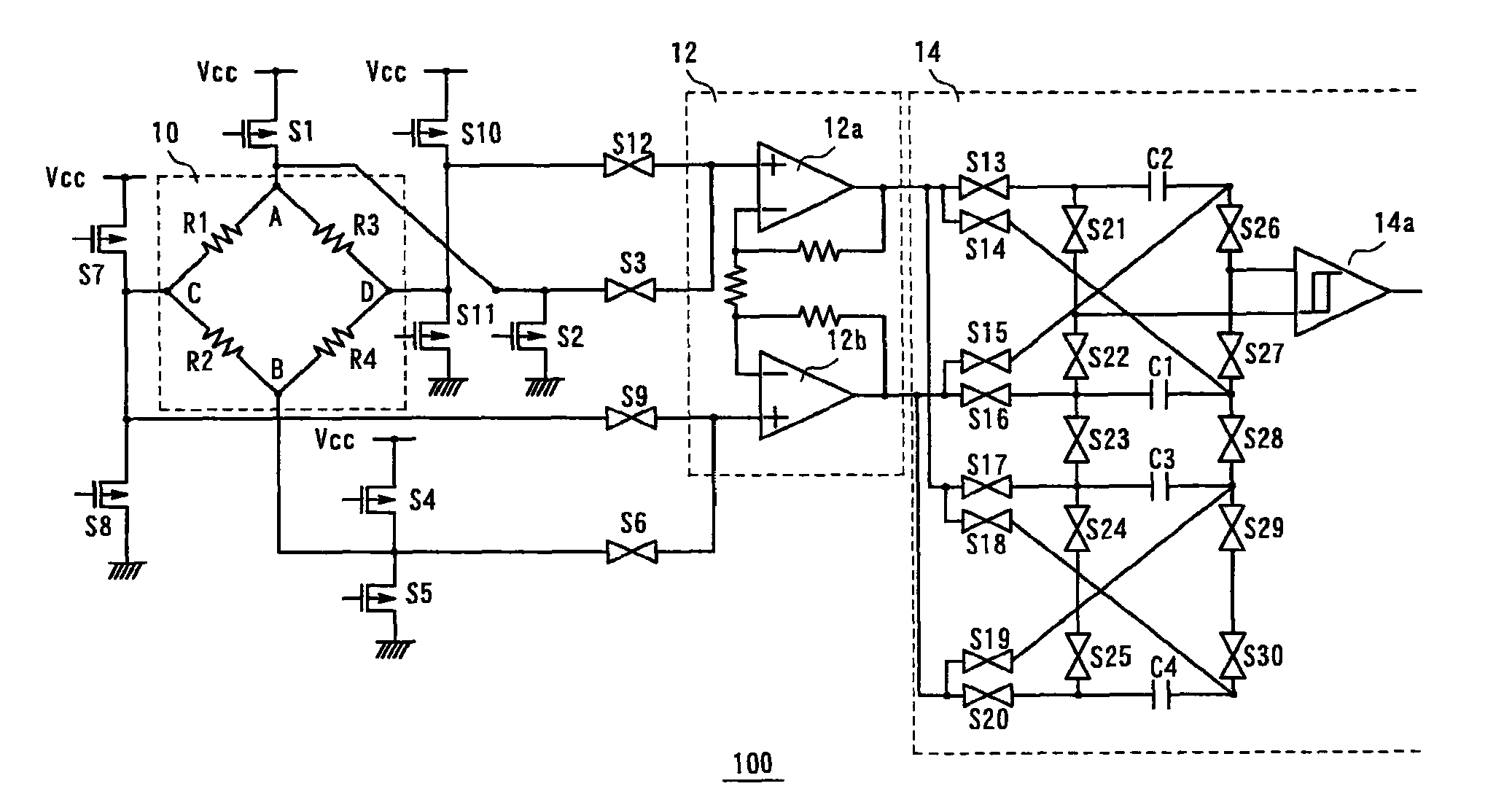
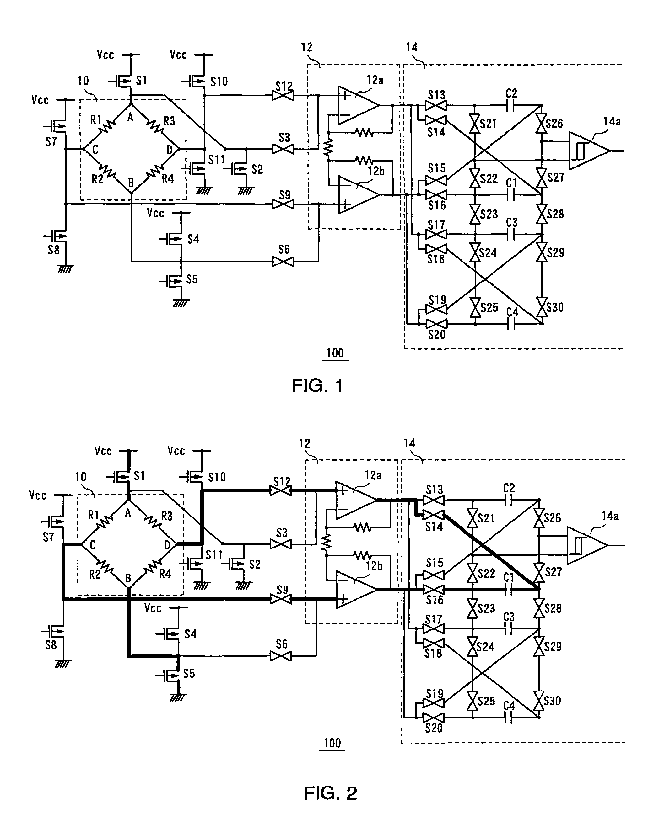
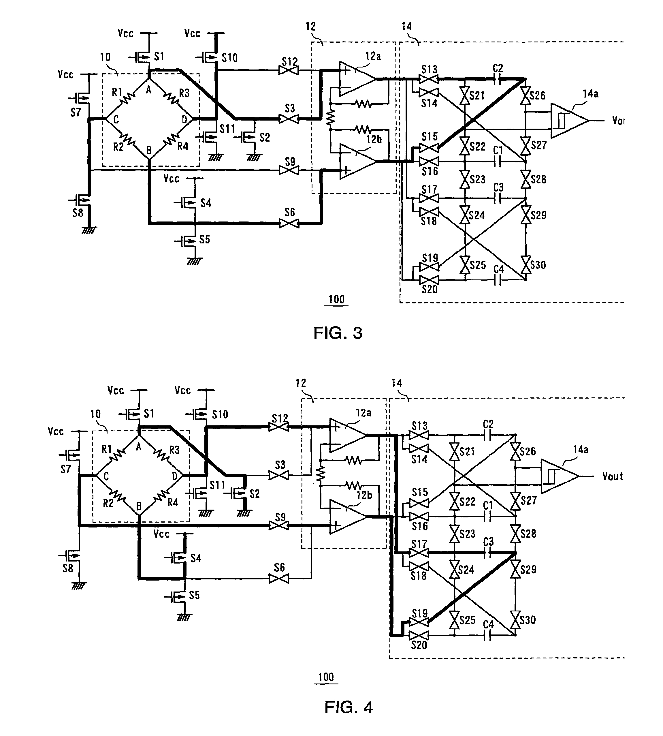
[0023]FIG. 1 shows a basic structure of an offset cancelling circuit (OC circuit) 100 of a Hall element. The offset cancelling circuit 100 comprises a Hall element 10, an amplifier circuit 12, and an averaging circuit 14.

[0024]The Hall element 10 can be represented as a bridge circuit of resistors R1˜R4. Switching elements S1˜S12 which switch connection points A˜D of the resistors R1˜R4 to a power supply voltage Vcc, ground, or output are connected to the resistors R1˜R4.

[0025]The amplifier circuit 12 comprises operational amplifiers 12a and 12b. The operational amplifier 12a amplifies a voltage which is input to a non-inverting input terminal (+) and outputs the amplified voltage. The operational amplifier 12b amplifies a voltage which is input to a non-inverting input terminal (+) and outputs the amplified voltage.

[0026]The averaging circuit 14 comprises switching elements S13˜S30, capacitors C1˜C4, and an operational amplifier 14a (which may be of a Schmitt buffer type). As shown...


PUM


Abstract

In an offset cancelling circuit of a Hall element, a voltage is applied from four directions and from outside such that a current flowing in the Hall element is switched by 90°, to set a first state through a fourth state, and output voltages of the Hall element in the first state through the fourth state are averaged.

Description

CROSS-REFERENCE TO RELATED APPLICATIONS[0001]The entire disclosure of Japanese Patent Application No. 2009-136907 filed on Jun. 8, 2009, including specification, claims, drawings, and abstract, is incorporated herein by reference in its entirety.BACKGROUND[0002]1. Technical Field[0003]The present invention relates to an offset cancelling circuit which is used for adjustment of an output or the like of a Hall element.[0004]2. Related Art[0005]In recent years, image capturing devices such as a digital still camera and a digital video camera realize higher image quality by increasing the number of pixels of an image capturing element of the image capturing device. On the other hand, as another method for realizing higher image quality of the image capturing device, it is desired to equip the image capturing device with a vibration absorption control circuit having a shake correction function in order to prevent shaking of imaging target caused by shaking of the hand holding the image c...

Claims


Application Information

Patent Timeline
Patent Type & Authority Patents(United States)
IPC IPC(8): G01R33/06G01D5/14G01R33/07H01L43/06
CPCG01B7/003G01B7/30G01D3/032G01D5/142G01R33/0035G01R33/07G01R33/072
Inventor OGAWA, TAKASHITERAZAWA, HIRONORINAKAI, TAKAHISA
Owner SEMICON COMPONENTS IND LLC
Why Eureka
Try Eureka