Photodiode having a buried well region

a photodiode and well-buried technology, applied in the field of photodiode pixel sensors, can solve the problems of reducing the collection efficiency of the photodiode, undesirably increasing the size of the pixel, and conventional pixel sensors may be limited in their collection efficiency and accuracy

Active Publication Date: 2013-08-20
NVIDIA CORP
View PDF12 Cites 7 Cited by
  • Summary
  • Abstract
  • Description
  • Claims
  • Application Information

AI Technical Summary

Benefits of technology

[0012]An embodiment of the imaging device includes at least two adjacent photodiode pixel sensors each including a buried region of opposite conductivity type than the semiconductor substrate in wh

Problems solved by technology

The inclusion of such active devices, however, may undesirably increase the size of a pixel and reduce the collection efficiency of the photodiode.
In addition, conventional pixel sensors may be limited in their collection efficiency and accuracy by their architecture, regardless of whether active devices are included.
In particular, some conventional photodiode pixel sensor architectures are susceptible to having photon-generated electrons recombine within the semiconductor substrate before being collected by the photodiode.
In addition, some conventional photodiode pixel sensor architectures lack sufficient isolation between adjacent pixels, allowing electrons g

Method used


Image

  • Photodiode having a buried well region
  • Photodiode having a buried well region
  • Photodiode having a buried well region

Examples


Embodiment Construction

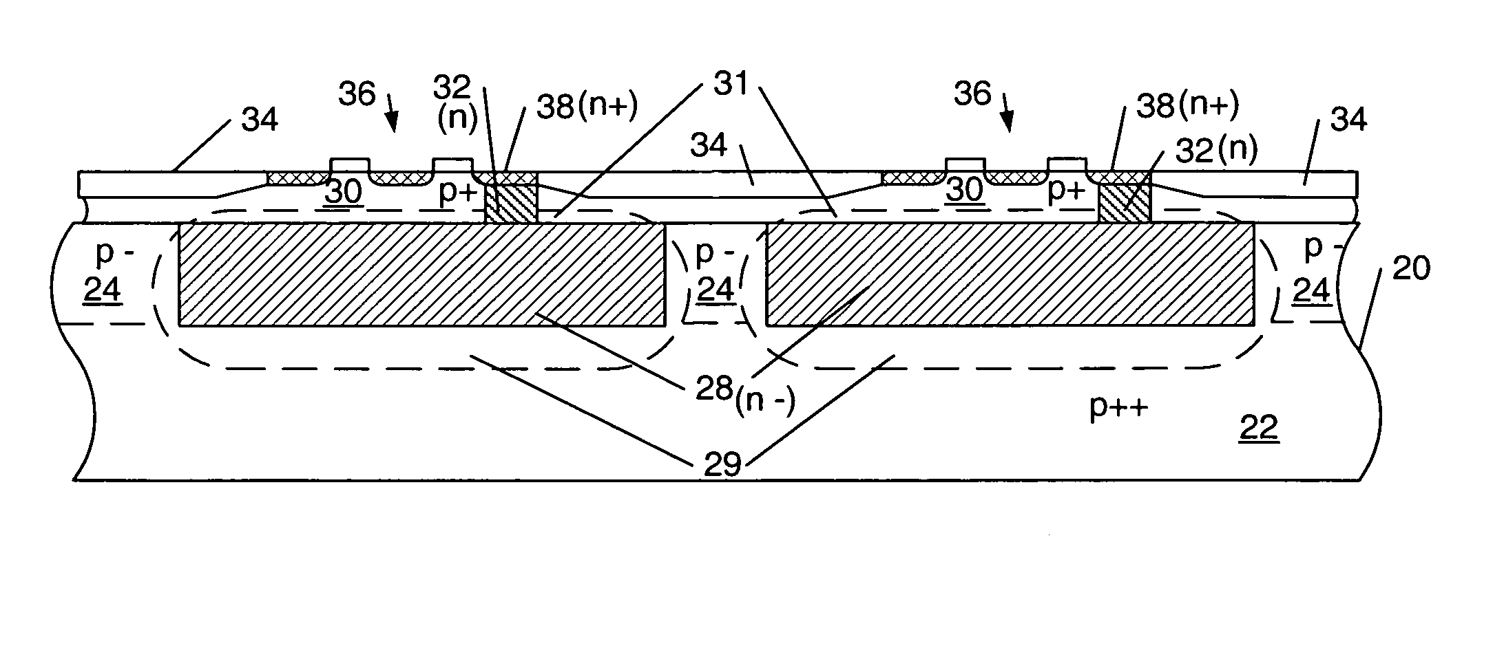
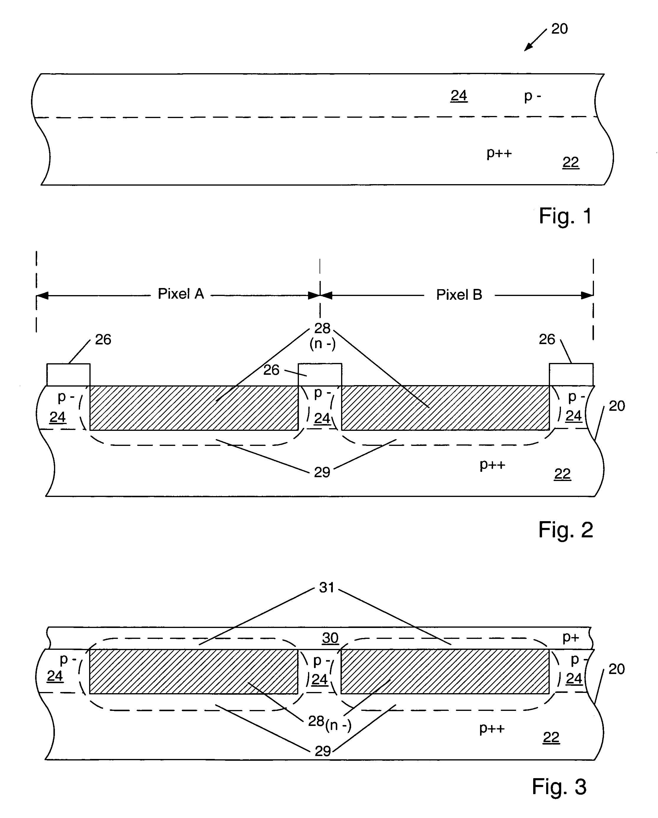
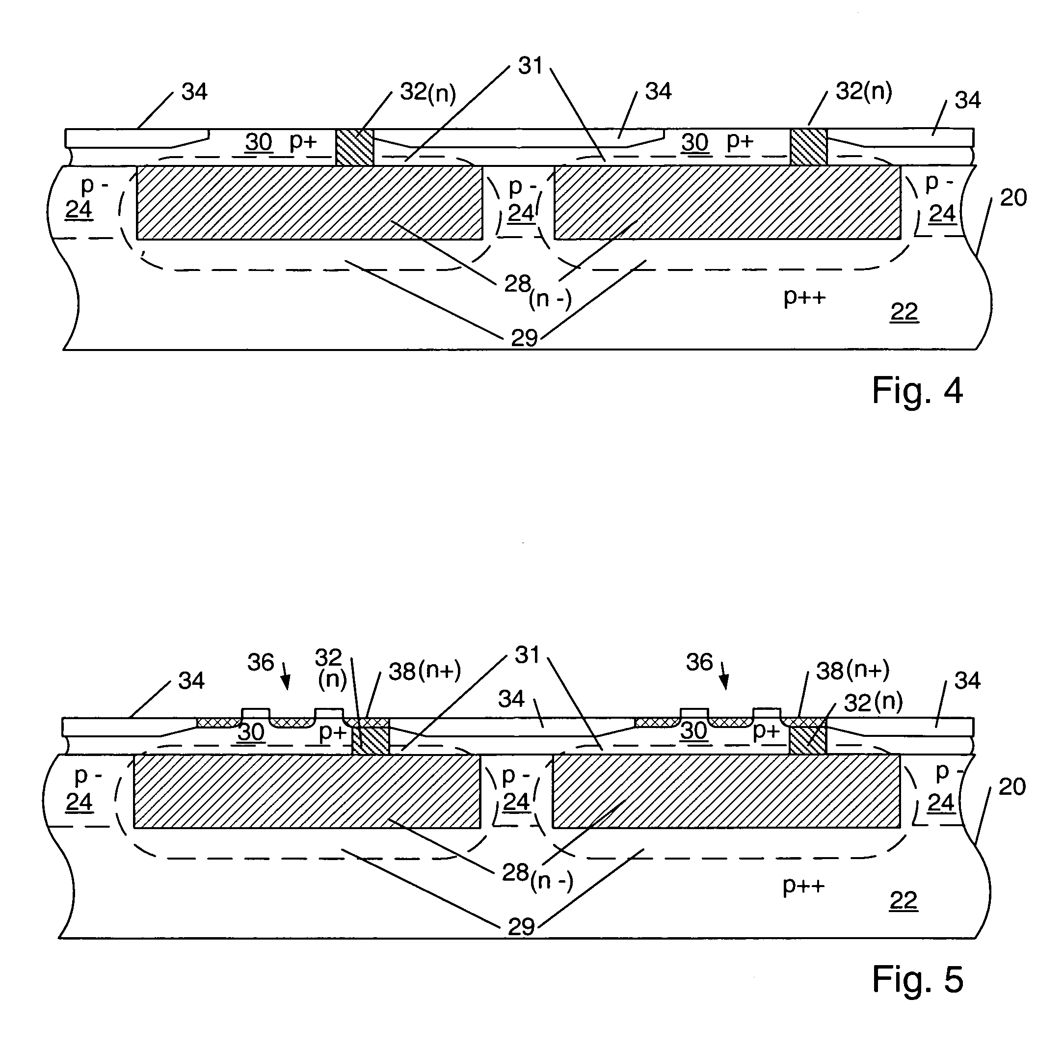
[0020]Turning to the drawings, an exemplary method is provided for forming an exemplary photodiode pixel sensor with a buried region of opposite conductivity type than a semiconductor substrate in which the photodiode is formed. As will be described in more detail below, such a photodiode pixel sensor architecture may advantageously reduce dark current as well as reduce the recombination and loss of photon generated carrier charge due to scattering of electrons. As a result, the photodiode pixel sensor described herein may have higher photon collection efficiency and improved image clarity as compared to conventional photodiode pixel sensors. Furthermore, the photodiode pixel sensor architecture described herein may incorporate active semiconductor devices without increasing the size of the pixel and / or hindering the collection efficiency of the photodiode relative to conventional photodiode pixel sensors.

[0021]FIG. 1 illustrates an exemplary semiconductor topography which may be us...


PUM


Abstract

A photodiode pixel sensor is provided having a buried region of opposite conductivity type than a semiconductor substrate in which the sensor is formed. The photodiode pixel sensor further includes a well region arranged upon and in contact with an upper surface of the buried region and a collection-junction extending into the well region. The well region and collection-junction are of the same conductivity type as the buried region and include greater net concentrations of dopants than the buried region and the well region, respectively. Such a configuration creates a drift field to channel (i.e., funnel) charge to the collection-junction. In some cases, the collection-junction may be a drain region of a transistor spaced above the buried region. An imaging device is also provided which includes at least two adjacent photodiode pixel sensors each including the aforementioned architecture isolated from each other by a distance less than approximately 2.0 microns.

Description

PRIORITY APPLICATION[0001]The present application claims priority to provisional application No. 60 / 609,636 entitled “Funnel Photodiode” filed Sep. 14, 2004.BACKGROUND OF THE INVENTION[0002]1. Field of the Invention[0003]The present invention relates generally to semiconductor based photon detectors and, more specifically, to photodiode pixel sensors.[0004]2. Description of the Related Art[0005]The following descriptions and examples are given as background information only.[0006]Sensors used for detecting electromagnetic radiation (a.k.a., photons) are generally referred to as pixel sensors and are widely fabricated within semiconductor-based materials for applications including but not limited to optical pointing devices and imaging arrays. Semiconductor based pixel sensors commonly employ photodiodes as sensing elements and, in some cases, include a number of active semiconductor devices, such as transistors, to amplify the charge that is collected in a light sensitive element or...

Claims


Application Information

Patent Timeline
IPC IPC(8): H01L31/0352
CPCH01L27/14638H01L31/035272H01L31/103H01L27/14607
Inventor JENNE, FREDRICK B.
Owner NVIDIA CORP
Why Eureka
Try Eureka