Integrated field emission array for ion desorption

a field emission array and ion desorption technology, applied in the field of field emission arrays, can solve problems such as catastrophic failure, and achieve the effects of increasing the ratio of the field at the tip to the field at the gate, high electric field, and maximizing the ratio of the gate radius to the tip radius

Active Publication Date: 2013-09-17
NAT TECH & ENG SOLUTIONS OF SANDIA LLC
View PDF6 Cites 4 Cited by
  • Summary
  • Abstract
  • Description
  • Claims
  • Application Information

AI Technical Summary

Benefits of technology

[0004]The present invention is embodied in an integrated field emission array for ion desorption. Field emission arrays that are used for ion desorption typically operate at high applied voltages. The large electric fields can lead to dielectric breakdown or electron emission from the gate, both of which may result in catastrophic failure. To create a high electric field at the tip while suppressing electron emission from the gate, the ratio of gate radius to tip radius is maximized to the extent that fabricati...

Problems solved by technology

The large electric fields can lead to dielectric breakdown or electro...

Method used


Image

  • Integrated field emission array for ion desorption
  • Integrated field emission array for ion desorption
  • Integrated field emission array for ion desorption

Examples


Embodiment Construction

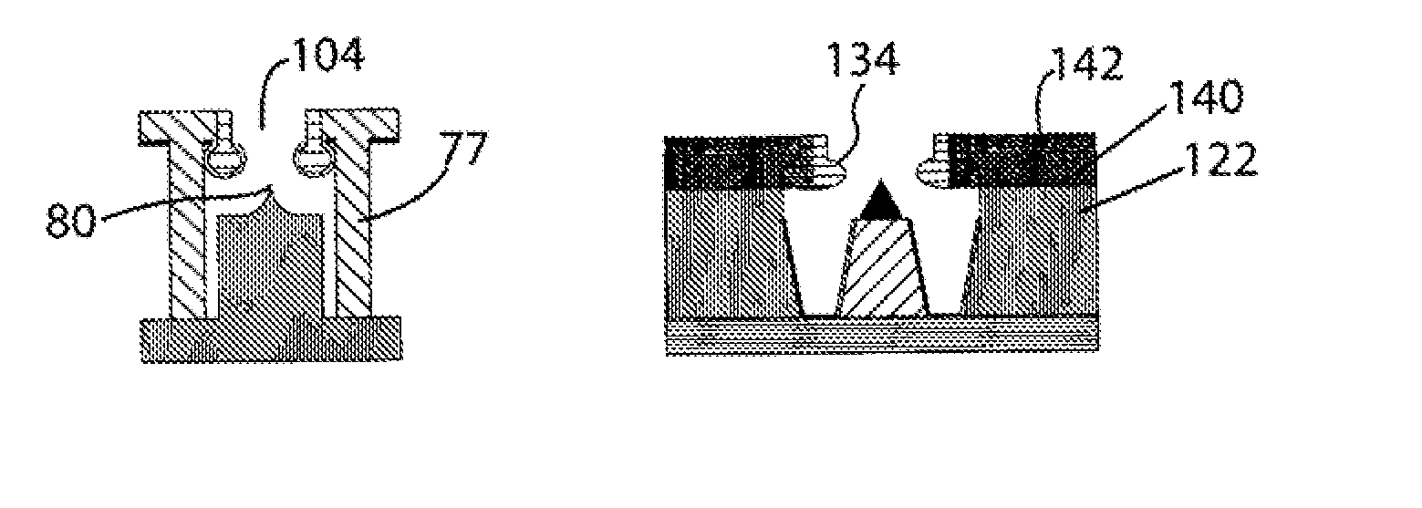
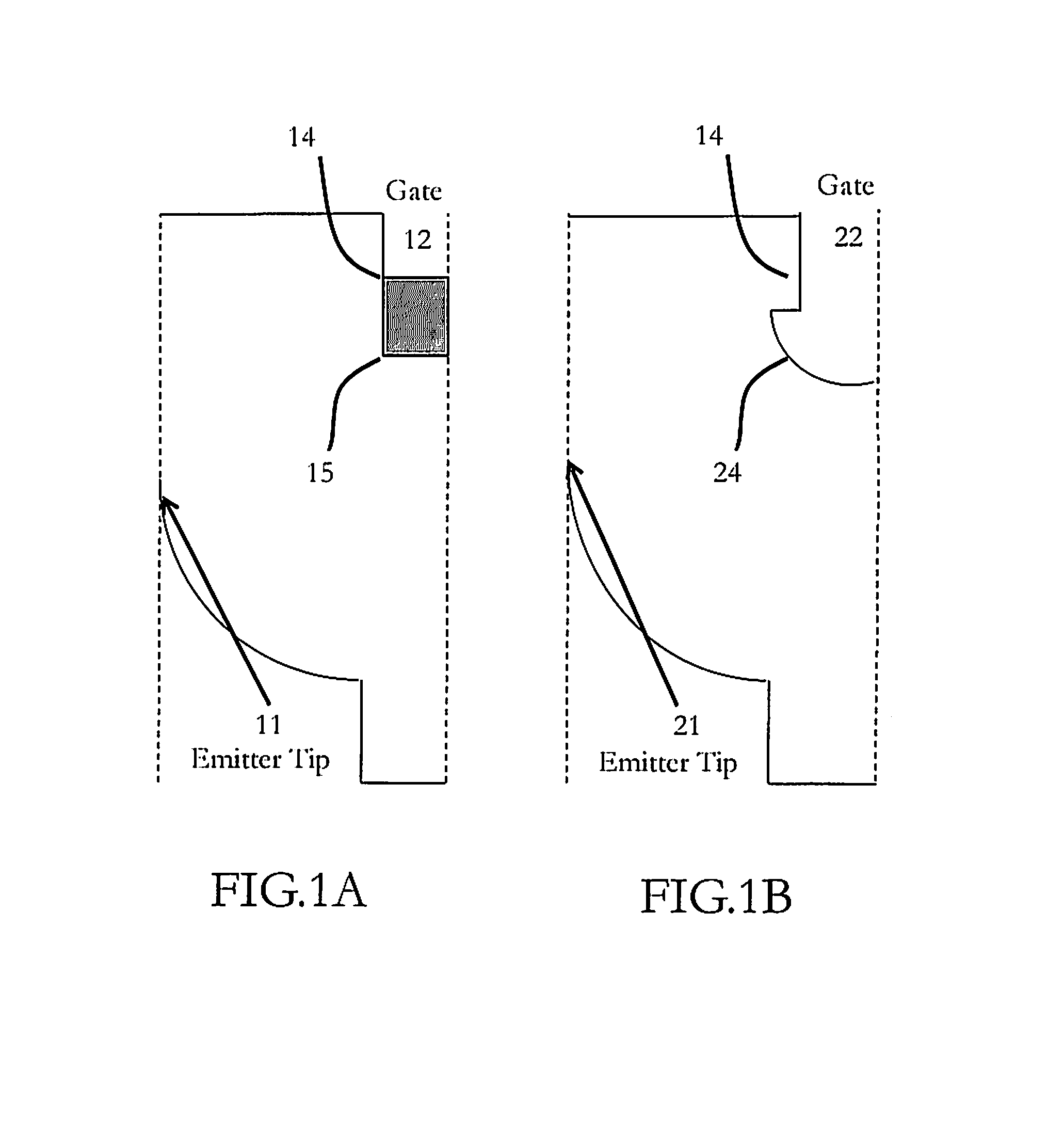
[0017]Field emission arrays (FEAs) have traditionally been fabricated using relatively simple thin film methods. See C. A Spindt, J. Appl. Phys. 39 (7), 3504 (1968); and C. A. Spindt et al., IEEE Trans. Electron Devices 38 (10), 2355 (1991). The elegance of this approach is undeniable, but it may not be suitable for high voltage field ionization or desorption sources. High voltage devices use a thick dielectric between the gate and substrate, which can be difficult to accommodate with thin film methods. In reverse-bias operation for field desorption (or ionization), it is desirable to suppress electron emission from the gate and which may cause special consideration to be given to the shape and position of the gate.

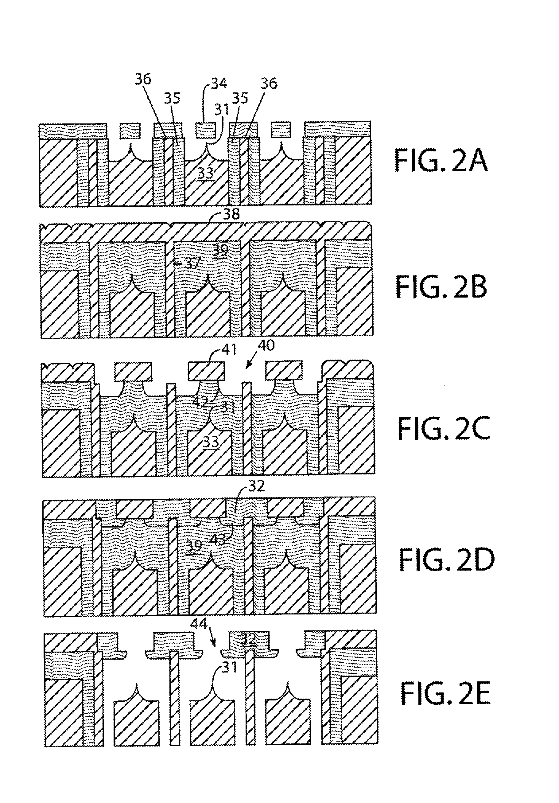
[0018]Therefore, a need remains for ion desorption sources that can, be fabricated using surface micromachining and related technologies. The additional complexity enabled by these methods allows for fabrication of arrays that can sustain high voltage and produce the high...


PUM


Abstract

An integrated field emission array for ion desorption includes an electrically conductive substrate; a dielectric layer lying over the electrically conductive substrate comprising a plurality of laterally separated cavities extending through the dielectric layer; a like plurality of conically-shaped emitter tips on posts, each emitter tip/post disposed concentrically within a laterally separated cavity and electrically contacting the substrate; and a gate electrode structure lying over the dielectric layer, including a like plurality of circular gate apertures, each gate aperture disposed concentrically above an emitter tip/post to provide a like plurality of annular gate electrodes and wherein the lower edge of each annular gate electrode proximate the like emitter tip/post is rounded. Also disclosed herein are methods for fabricating an integrated field emission array.

Description

STATEMENT OF GOVERNMENT INTEREST[0001]This invention was made with Government support under contract no. DE-AC04-94AL85000 awarded by the U.S. Department of Energy to Sandia Corporation. The Government has certain rights in the invention.FIELD OF THE INVENTION[0002]The present invention relates to field emission arrays and, in particular, to an integrated field emission array for ion desorption and methods to fabricate the array.BACKGROUND OF THE INVENTION[0003]Field emission arrays (FEA) for ion desorption present unique challenges for microfabrication. Unlike arrays that are used for field emission of electrons, devices that are designed for ion emission desirably support the high voltages needed to achieve electrostatic field desorption. See C. A. Spindt et al., IEEE Trans. Electron Devices 38 (10), 2355 (1991). The onset of field ionization occurs when the field at the tip reaches about 10 V / nm, which is about 10 times greater than the field required for electron emission. Ion d...

Claims


Application Information

Patent Timeline
IPC IPC(8): H01L29/06
CPCH01J3/04H01J9/02H01L21/31111
Inventor RESNICK, PAUL J.HERTZ, KRISTIN L.HOLLAND, CHRISTOPHERCHICHESTER, DAVIDSCHWOEBEL, PAUL
Owner NAT TECH & ENG SOLUTIONS OF SANDIA LLC
Why Eureka
Try Eureka