Inspection apparatus

a technology of inspection apparatus and inspection chamber, which is applied in the field of inspection apparatus, can solve the problems of improving throughput, difficult to use refractive optics, and difficult to use in the wide wavelength band of first related art, and achieves the effects of simplifying optics, high throughput and high sensitivity inspection, and reducing the number of optical elements

Inactive Publication Date: 2013-09-24
HITACHI HIGH-TECH CORP
View PDF11 Cites 1 Cited by
  • Summary
  • Abstract
  • Description
  • Claims
  • Application Information

AI Technical Summary

Benefits of technology

[0013]An object of the present invention is to provide an inspection apparatus having high throughput and high sensitivity with respect to a number of various manufacturing processes and defects of interest.
[0035]According to one aspect of the present invention, a sufficiently large longer-side size is secured in a field of view in non-straight-line slit form by using a reflective optics aberration-corrected in a wide wavelength band, and optimum wavelength bands are selected according to a number of various manufacturing processes and defects, thus enabling high-throughput and high-sensitivity inspection. According to another aspect of the present invention, the number of optical elements can be reduced and the effect of simplifying the optics can be obtained.

Problems solved by technology

However, the first related art has a problem of being difficult to use in a wide wavelength band because the refractive optics has a chromatic aberration.
There is also a problem that the absorption by lenses in the vacuum ultraviolet region is large, and therefore, it is presently impossible to use the refractive optics.
The second related art satisfies the second condition but has a problem in improving the throughput.

Method used


Image

  • Inspection apparatus
  • Inspection apparatus
  • Inspection apparatus

Examples


embodiment 1

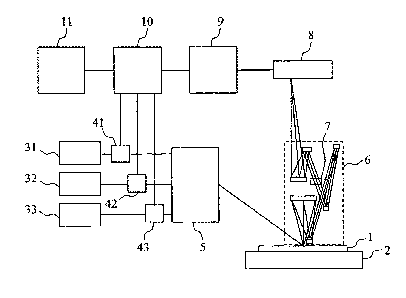
[0073]A dark-field inspection apparatus for inspecting a semiconductor wafer will be described as an embodiment of the present invention. FIG. 1 schematically shows the construction of the inspection apparatus. Main components of the apparatus are a stage 2 on which a wafer 1 is mounted, a visible light laser 31, an ultraviolet laser 32, a deep ultraviolet laser 33, attenuators 41, 42, and 43, an illumination optics 5, a reflective optics 6, a spatial filter 7, an image sensor 8, an image processing system 9, a control system 10, and an input-output operation system 11.

[0074]When the wafer 1 is loaded in the inspection apparatus, an operator inputs information on the manufacturing process and a defect of interest to the input-output operation system 11. The control system 10 selects an optimum wavelength band such as described below by using this information and referring to a database accumulated in advance through a simulation or an experiment. The lasers 31, 32, and 33 emit light...

embodiment 2

[0092]An embodiment of the present invention preferable in a case where a plurality of defects of interest exist on a wafer will be described with reference to FIG. 6. The same reference numerals as those in FIG. 1 denote identical or corresponding components. In this embodiment, diffractive-optical elements 16 are disposed on the exit side of the reflective optics 6 to separate light into wavelength bands. As each diffractive-optical element, a diffraction grating, a prism or the like can be used. Separated light is imaged on an image sensor 81 and an image sensor 82 in correspondence with the wavelength bands. An optimum wavelength band can be selected with respect to each detect of interest. Therefore, an image of a high signal-to-noise ratio can be obtained.

embodiment 3

[0093]Another embodiment of the present invention will be described with reference to FIG. 7. The same reference numerals as those in FIG. 1 denote identical or corresponding components. In this embodiment, a lamp 17 which emits light in a wide wavelength band from a visible light region to a deep ultraviolet region is used as a light source, and a wavelength filter 18 allows light in a predetermined wavelength band to pass through. The lamp has a lower output per wavelength band in comparison with lasers but is capable of making finer selections from wavelength bands because it emits a continuous spectrum of light. Finer selections from wavelength bands can be made in the wavelength filter 18 on the basis of a command from the control system 10. The present embodiment is highly effective in reducing the bad influence of thin-film interference. Also, the construction of the apparatus is simplified in comparison with a case where a plurality of lasers are incorporated.


PUM

PropertyMeasurementUnit
sizeaaaaaaaaaa
wavelengthaaaaaaaaaa

Abstract

The present invention provides an inspection apparatus having a high throughput and high sensitivity with respect to a number of various manufacturing processes and defects of interest in inspection of a specimen such as a semiconductor wafer on which a pattern is formed. The apparatus illuminates with light the specimen having the pattern formed thereon, forms an image of the specimen on an image sensor through a reflective optics, and determines the existence / nonexistence of a defect. The reflective optics has a conjugate pair of Fourier transform optics. An aberration of the reflective optics is corrected off-axis. The reflective optics has a field of view in non-straight-line slit form on the specimen surface. Also, the optics is of a reflection type, includes a conjugate pair of Fourier transform optics and has a field of view in non-straight-line slit form. An optimum wavelength band is selected according to the specimen (FIG. 1).

Description

BACKGROUND OF THE INVENTION[0001]1. Field of the Invention[0002]The present invention relates to an inspection apparatus for inspecting a specimen on which a pattern is formed, e.g., a wafer in manufacture of a semiconductor device and, more particularly, to an optics in an optical inspection apparatus.[0003]2. Background Art[0004]Manufacture of a semiconductor device is divided into a front end process and a back end process. The front end process includes isolation forming, well forming, gate forming, source / drain forming, interlayer dielectric film forming and planarization. In the back end process, contact plug forming, interlayer dielectric film forming, planarization and metal wiring forming are repeated and passivation film forming is finally performed. In the course of the above-described manufacturing process, wafers are extracted and inspection of defects is performed. The defects include foreign particles on the wafer surface, scratches in the wafer surface, and pattern d...

Claims


Application Information

Patent Timeline
Patent Type & Authority Patents(United States)
IPC IPC(8): G01N21/00G06V10/88
CPCG01N21/9501G01N21/95623G06K9/74G01N2021/8822G06V10/88
Inventor ITO, MASAAKINOGUCHI, MINORIMATSUI, SHIGERU
Owner HITACHI HIGH-TECH CORP
Why Eureka
Try Eureka