Semiconductor device with a balun

a technology of semiconductor devices and baluns, which is applied in the direction of semiconductor devices, semiconductor/solid-state device details, waveguides, etc., can solve the problems of imposing limitations in reducing the differential impedance zo, unable to be sufficiently narrow, and large losses of passive elements, such as transmission lines or inductors

Active Publication Date: 2013-11-05
PANASONIC CORP
View PDF17 Cites 6 Cited by
  • Summary
  • Abstract
  • Description
  • Claims
  • Application Information

AI Technical Summary

Benefits of technology

[0029]According to the present invention, it is possible to provide a semiconductor device having a wide-band and small-size balun. In the semiconductor device, only the electromagnetic coupling between the unbalanced line and the balanced lines of the balun can be increased without increasing the electromagnetic coupling between the lines other than the balun formed in different interconnect layers.

Problems solved by technology

However, there is a problem in that losses of passive elements, such as transmission lines or inductors, are large due to low resistance of the Si semiconductor substrate.
Thus, it is not possible to sufficiently narrow the space to an adjacent interconnect film, thereby imposing limitations in decreasing the differential impedance Zo.

Method used


Image

  • Semiconductor device with a balun
  • Semiconductor device with a balun
  • Semiconductor device with a balun

Examples


Embodiment Construction

[0044]Hereinafter, an embodiment of the present invention is described with reference to the drawings.

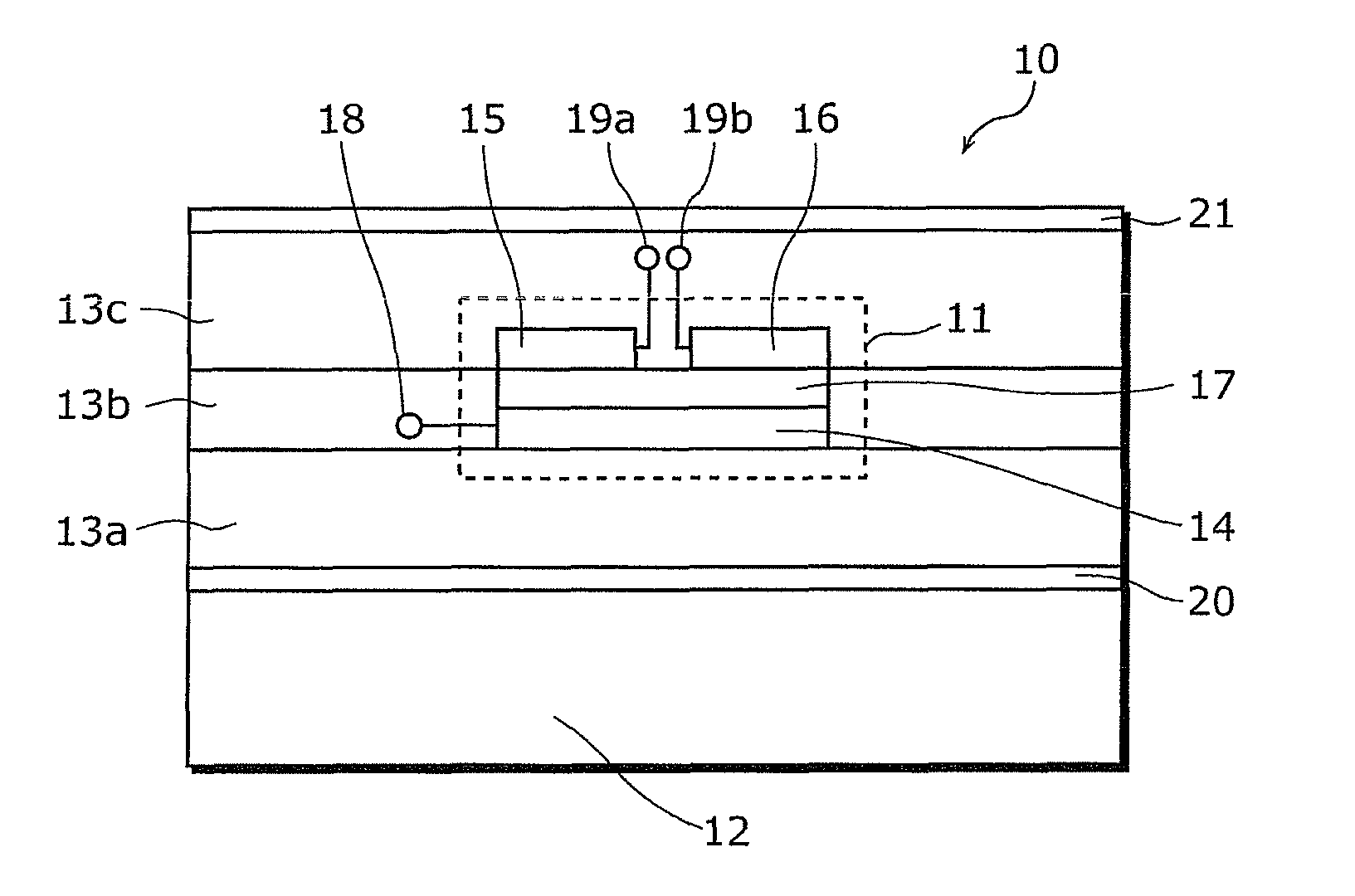
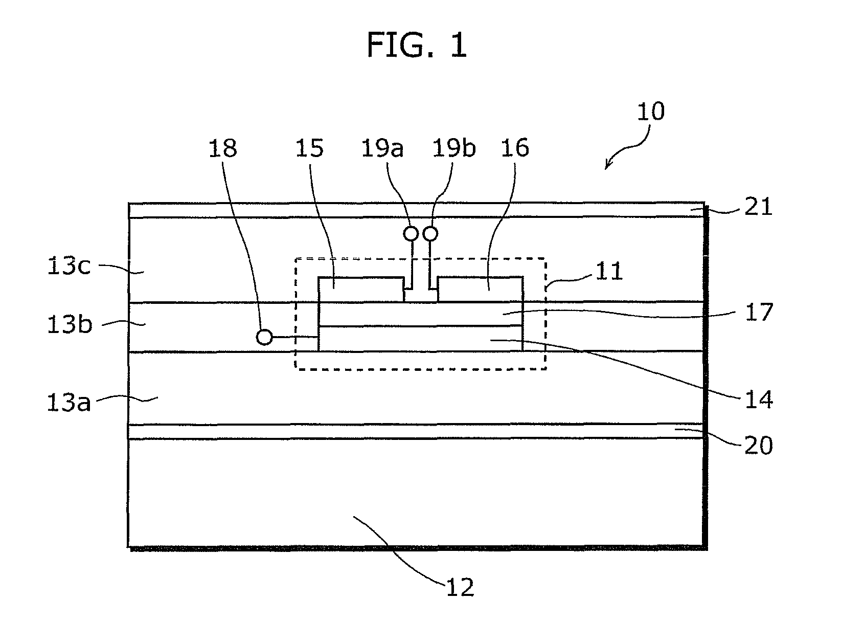
[0045]FIG. 1 is a cross sectional view showing an example of a structure of a semiconductor integrated circuit device 10 including a balun 11 according to the embodiment of the present invention.

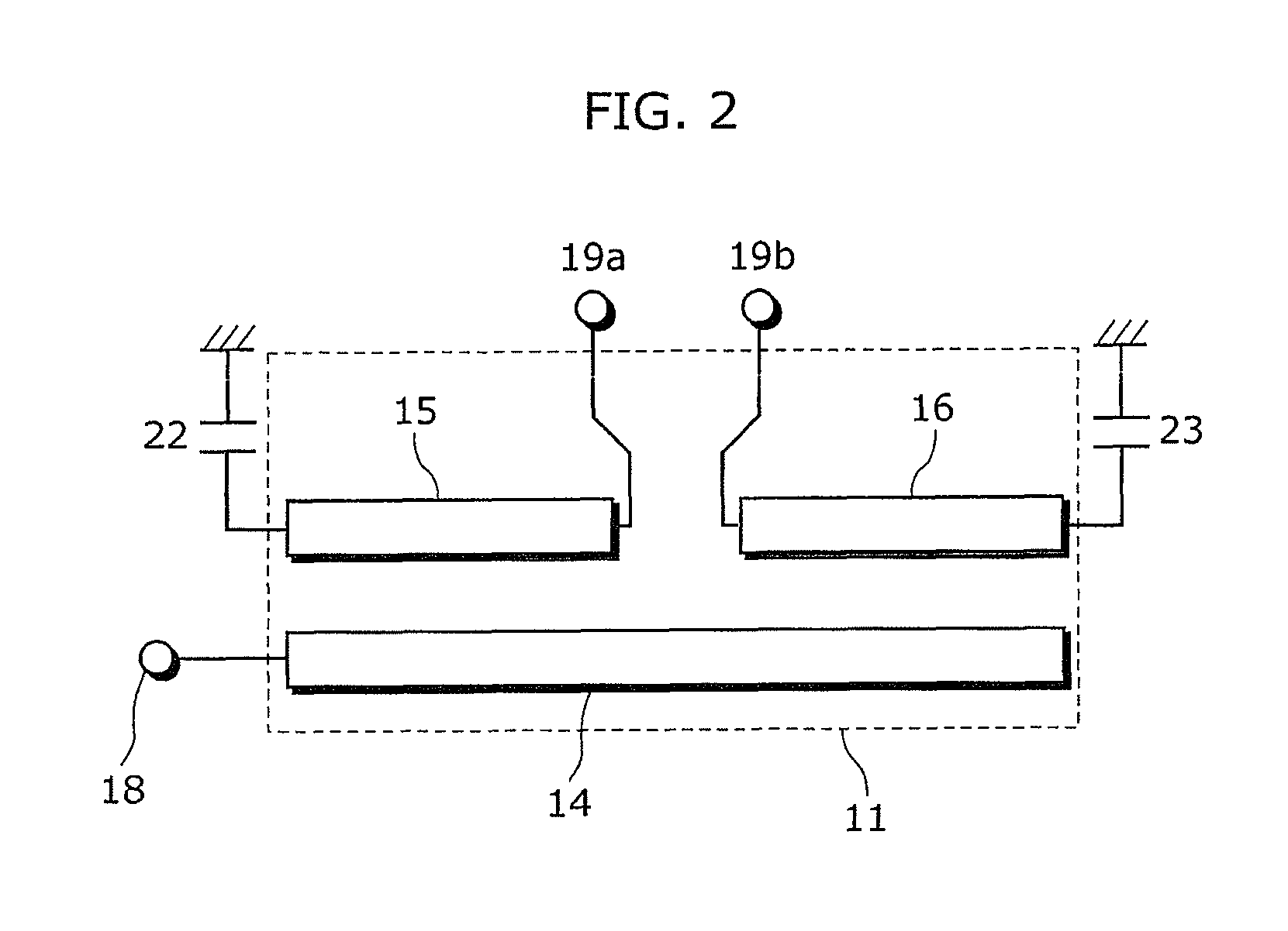
[0046]FIG. 2 is a circuit diagram showing a circuit structure of the balun 11 shown in FIG. 1.

[0047]The semiconductor integrated circuit device 10 shown in FIG. 1 includes: the balun 11, a semiconductor substrate 12, dielectric films 13a, 13b, and 13c, an unbalanced line 14 for transmitting an unbalanced signal, balanced lines 15 and 16 for transmitting a balanced signal, a nano-composite film (a high dielectric film) 17, an unbalanced signal input (output) terminal 18, balanced signal output (input) terminals 19a and 19b, and ground electrode films 20 and 21.

[0048]Above the semiconductor substrate 12, dielectric layers where dielectric films are provided and interconnect layers where interc...


PUM


Abstract

A semiconductor integrated circuit device with a balun which is formed above a conductive semiconductor substrate and which includes a dielectric film, an unbalanced line for transmitting an unbalanced signal, and balanced lines for transmitting a balanced signal. The unbalanced line is placed opposite to the balanced lines via a nano-composite film that is a region of the dielectric film. The nano-composite film, interposed between the unbalanced line and the balanced lines, has a relative permittivity higher than that of other regions of the dielectric film. This allows suppression of electromagnetic coupling of transmission lines or passive elements other than the balun, thereby providing a semiconductor device with a wide-band and small-size balun.

Description

TECHNICAL FIELD[0001]The present invention relates to a semiconductor device with a balun miniaturized to be mounted on a Monolithic Microwave Integrated Circuit (MMIC) chip in a radio-frequency semiconductor device such as various types of communications apparatuses and radars.BACKGROUND ART[0002]A balun is used for converting an unbalanced signal, transmitting through an unbalanced transmission line, to a balanced signal, transmitting through a balanced transmission line and vice versa. The balun is also capable of performing impedance conversion. For example, in the case where an unbalanced signal is provided to an unbalanced terminal of the balun, a pair of balanced signals, having phases that are different by 180 degrees (reverse phase) and having the same amplitude, are output through a balanced terminal of the balun. Further, the balun may also be formed in inner interconnection layers within a semiconductor chip.[0003]A balun that can be used for GHz is available which is fa...

Claims


Application Information

Patent Timeline
Patent Type & Authority Patents(United States)
IPC IPC(8): H01L23/58
CPCH01L23/64H01L23/66H01P5/10H01L2924/19104H01L2924/3011H01L2924/0002H01L2924/00
Inventor UJITA, SHINJIFUKUDA, TAKESHISAKAI, HIROYUKI
Owner PANASONIC CORP
Why Eureka
Try Eureka