

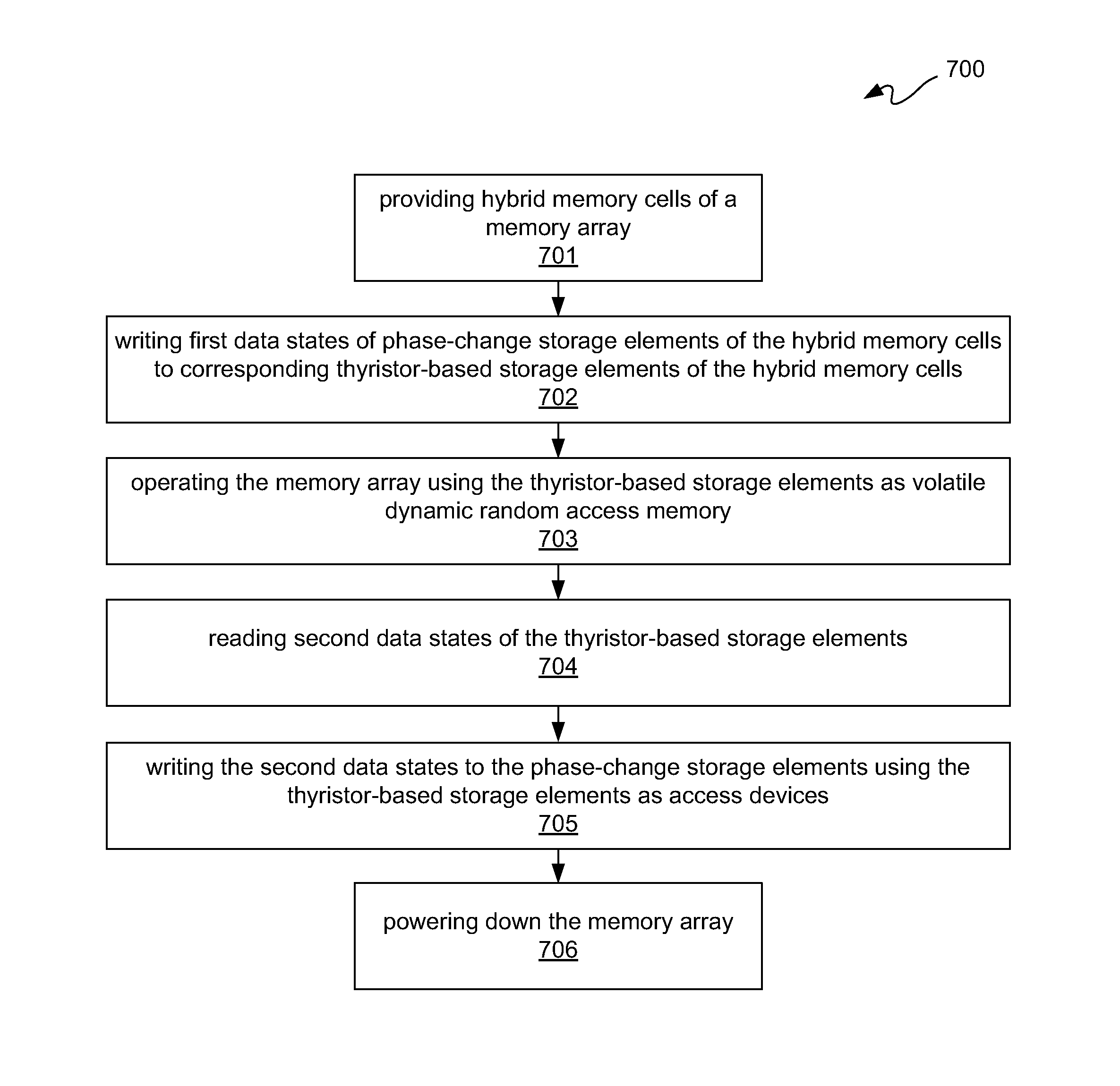
Hybrid memory cell array and operations thereof
a memory cell array and hybrid technology, applied in static storage, digital storage, instruments, etc., can solve the problems of affecting the restore rate of such cells, dram is relatively slow, and the access time is typically near 20 nanoseconds
- Summary
- Abstract
- Description
- Claims
- Application Information
AI Technical Summary
Benefits of technology
Problems solved by technology
Method used
Image

Examples
Embodiment Construction
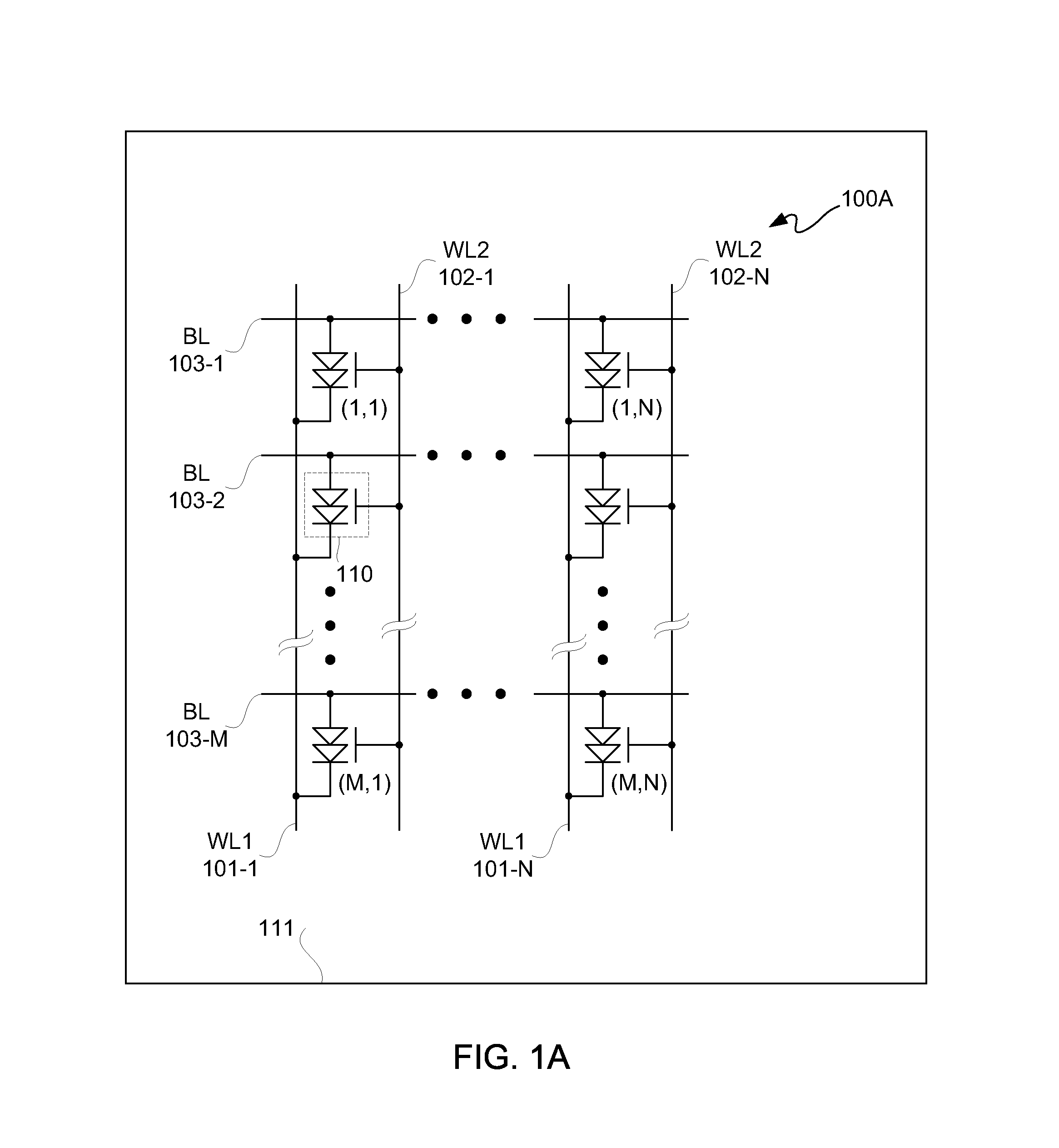
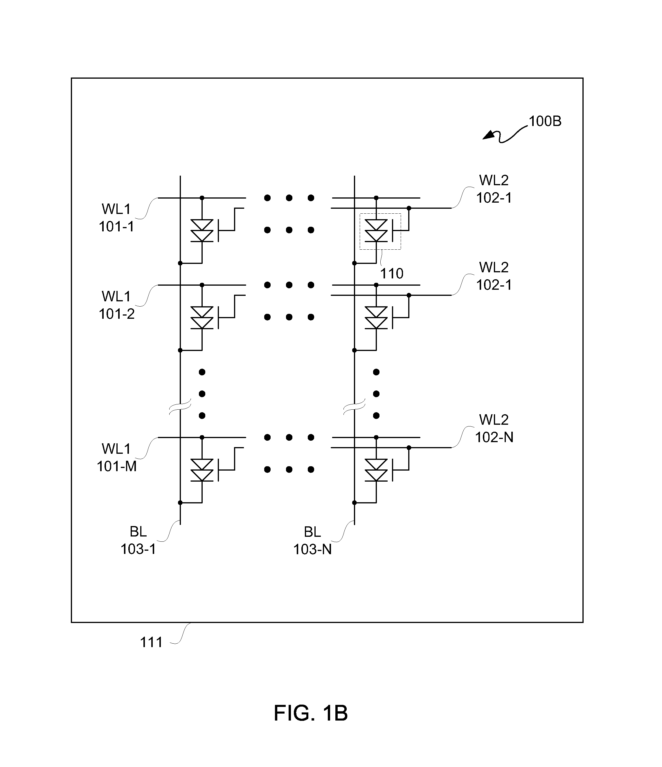
[0022]In the following description, numerous specific details are set forth to provide a more thorough description of the specific embodiments of the invention. It should be apparent, however, to one skilled in the art, that the invention may be practiced without all the specific details given below. In other instances, well-known features have not been described in detail so as not to obscure the invention. For ease of illustration, the same number labels are used in different diagrams to refer to the same items; however, in alternative embodiments the items may be different. Moreover, for purposes of clarity, a single signal or multiple signals may be referred to or illustratively shown as a signal to avoid encumbering the description with multiple signal lines. Moreover, along those same lines, a transistor, among other circuit elements, may be referred to or illustratively shown as a single transistor though such reference or illustration may be representing multiples thereof. F...
PUM
 Abstract
Description
Claims
Application Information