Placing heat sink into packaging by strip formation assembly

a technology of heat sink and packaging, applied in the field of integrated circuits, can solve the problems of not being able to accommodate the design of most packaging schemes, and affecting the thermal characteristics of packaged devices

Active Publication Date: 2013-11-12
MARVELL ASIA PTE LTD
View PDF3 Cites 10 Cited by
  • Summary
  • Abstract
  • Description
  • Claims
  • Application Information

AI Technical Summary

Benefits of technology

[0007]This disclosure also describes a method for building a packaged semiconductor device. The method comprising placing a plastic film in a compression mold and aligning a metal film over the plastic film. Next, a molding compound is dispersed over the metal film. Then, a lead frame assembly is aligned over the metal film and the lead frame assembly comprises a plurality of semiconductor devices. The semiconductor devices are compressed into the molding compound to (i) embed the metal film into the molding compound, and to (ii) prevent physical contact between the metal film and the lead frame.

Problems solved by technology

Thermal characteristics of packaged semiconductor devices have been a design issue with respect to device performance and reliability.
However, controlling thermal characteristics of packaged devices has been problematic due to the lack of space available to implement thermal conductivity solutions in an efficient manner.
Unfortunately, most packaging schemes cannot accommodate such a design.

Method used


Image

  • Placing heat sink into packaging by strip formation assembly
  • Placing heat sink into packaging by strip formation assembly
  • Placing heat sink into packaging by strip formation assembly

Examples


Embodiment Construction

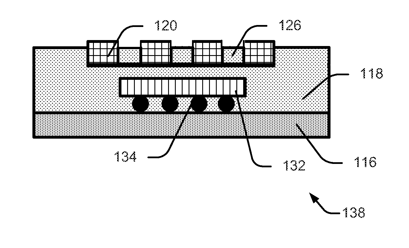
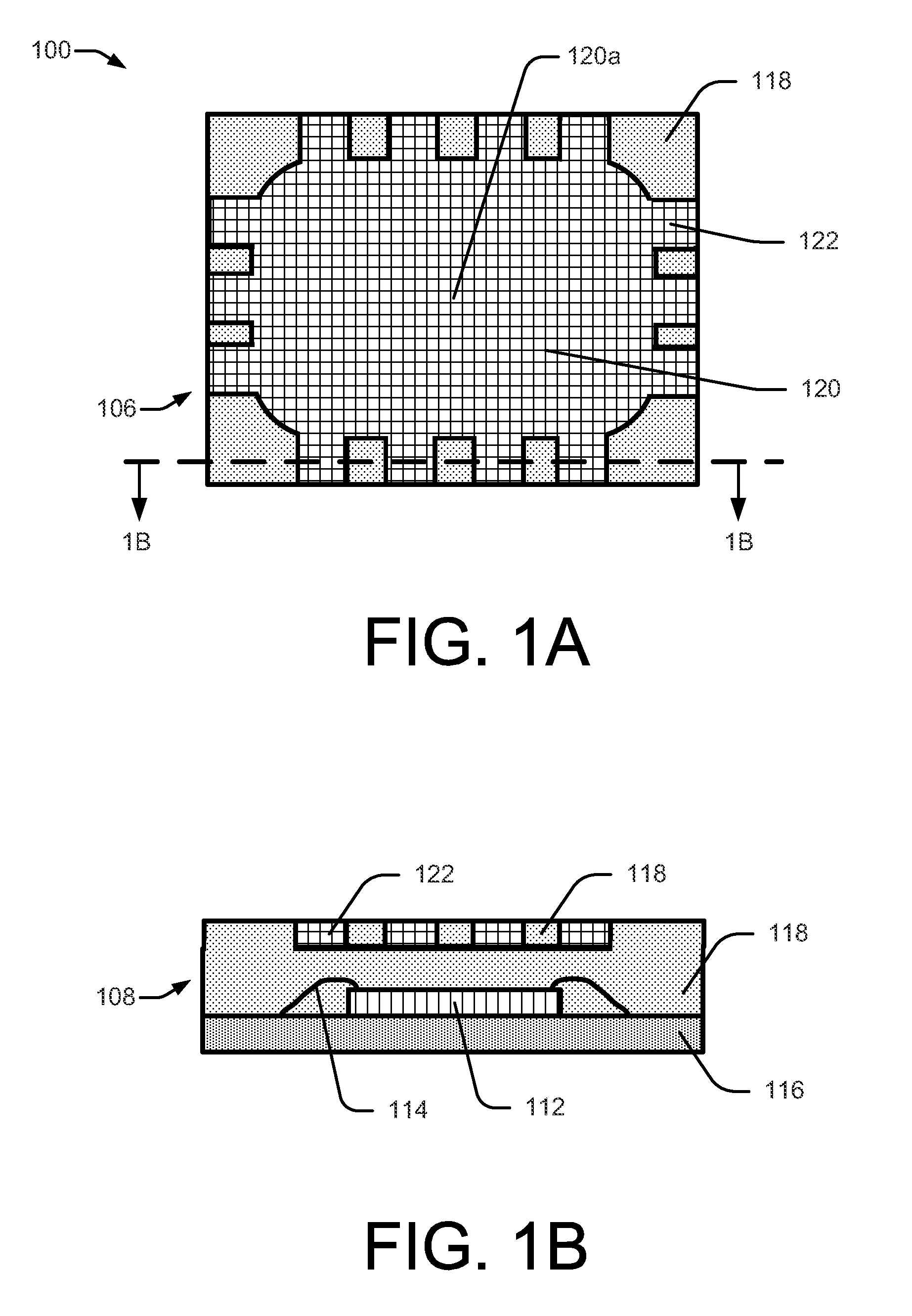
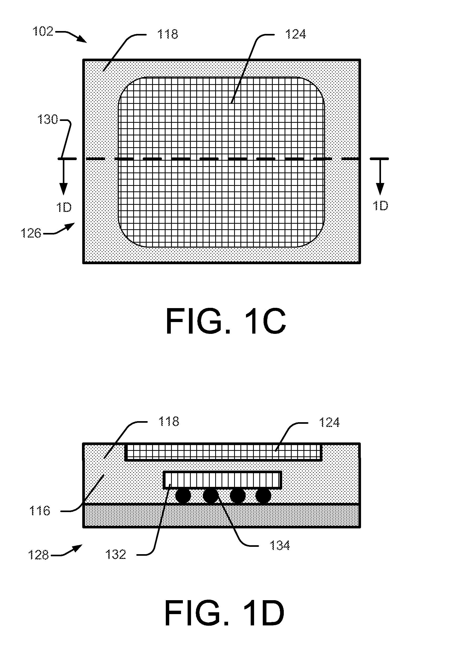
[0014]FIGS. 1A-1F illustrate top views and cross sectional views of a packaged wire bonded device 100, and two packaged flip-chip devices 102, 104 that have heat spreaders embedded in the molded portion of their packaging.

[0015]The packaged wire bonded device 100 is illustrated in top view in FIG. 1A and cross sectional view in FIG. 1B per cross section line 1B-1B of FIG. 1A. The packaged wire bonded device 100 includes a semiconductor device 112 that is wire bonded 114 to a substrate 116 or lead frame. The packaged wire bonded device 100 also includes molded insulating material 118, and a heat spreader 120 embedded in the molded insulating material 118. As can be seen in the top view of FIG. 1A, the heat spreader 120 covers a significant portion of the top surface of packaged wire bonded device 100, and (on one implementation) is arranged to have fingers 122 that protrude to the edge of the device 100. In one implementation, the fingers 122 increase the rigidity of the packaged wir...


PUM


Abstract

Embodiments of the present disclosure describe semiconductor device packaging techniques and devices that incorporate a heat spreader into the insulating material of a packaged semiconductor device. In one embodiment, a device comprising a semiconductor device is coupled to a substrate, and insulating material covers (i) a portion of the semiconductor device and (ii) a portion of the substrate. The device also comprises a heat spreader embedded in the insulating material and the heat spreader is isolated from the substrate at least in part by the insulating material.

Description

CROSS REFERENCE TO RELATED APPLICATIONS[0001]This disclosure claims priority to U.S. Provisional Patent Application No. 61 / 389,409, filed Oct. 4, 2010, and U.S. Provisional Patent Application No. 61 / 392,816, filed Oct. 13, 2010, the entire specifications of which are hereby incorporated by reference in their entireties for all purposes, except for those sections, if any, that are inconsistent with this specification.TECHNICAL FIELD[0002]Embodiments of the present disclosure relate to the field of integrated circuits, and more particularly, to techniques, structures, and configurations of semiconductor chip packaging.BACKGROUND[0003]The background description provided herein is for the purpose of generally presenting the context of the disclosure. Work of the presently named inventors, to the extent it is described in this background section, as well as aspects of the description that may not otherwise qualify as prior art at the time of filing, are neither expressly nor impliedly ad...

Claims


Application Information

Patent Timeline
Patent Type & Authority Patents(United States)
IPC IPC(8): H01L23/495H01L23/28
CPCH01L23/4334H01L24/97H01L23/3121H01L21/56H01L2224/16H01L2224/48091H01L2224/48247H01L2924/00014H01L2224/81H01L2224/97H01L2224/85H01L2924/181
Inventor CHEN, CHENDERLIU, CHENGLINLIOU, SHIANN-MING
Owner MARVELL ASIA PTE LTD
Why Eureka
Try Eureka